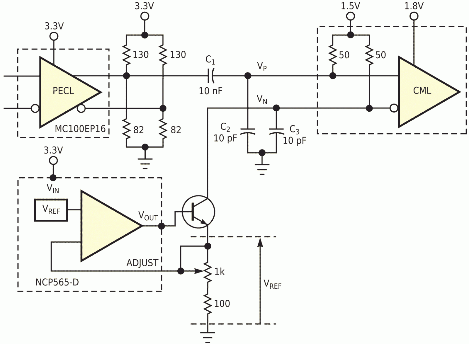
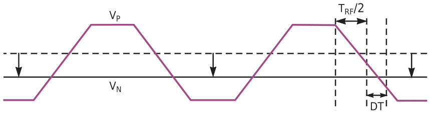
To test a gigabit-speed data-recovery chip, you need a clock with a controllable duty cycle. Because most pattern and clock generators have a fixed duty-cycle output of 50%, the design may require a small circuit to distort the duty cycle. The signal with controllable duty cycle drives a standard CML (current-mode-logic) input with on-chip termination resistors. One side, VP, of the differential CML input takes single-ended drive from a PECL (positive-emitter-coupled-logic) circuit (Figure 1). The other input, VN, connects to a controllable dc voltage. If this dc voltage is equal to the average voltage of the single-ended signal, the duty cycle stays 50%. If the signal has nonzero rise and fall times (TRF), you can distort the duty cycle by lowering the dc voltage (Figure 2). The distortion generated is equal to the time difference between the crossing of the single-ended signal and its average and the crossing between the single-ended signal and the set dc voltage (DT). Thus, the theoretical maximum distortion that you can generate is TRF.
 |
|
| Figure 1. | This circuit can make slight adjustments to the duty cycle you apply to a CML input. |
You can control TRF by selecting a buffer with the desired TRF value, the MC100EP16 buffer in this design, and by changing the output capacitance for this buffer (C2). To set the voltage at node VN, the design uses the internal termination resistors and a controllable current source instead of applying a dc voltage source. This procedure makes the circuit more immune to power-supply changes. Because the single-ended signal is ac-coupled, the average voltage of this signal at node VP is equal to the internal termination voltage of the CML input. If no current enters the VN input, this node also assumes the internal termination voltage, and the duty cycle is 50%. This voltage is independent of the average voltage of the single-ended signal at the buffer's output and the internal termination voltage.
 |
|
| Figure 2. | By exploiting the rise and fall time of a signal and manipulating a dc bias voltage, you can control the duty cycle of a CML signal. |
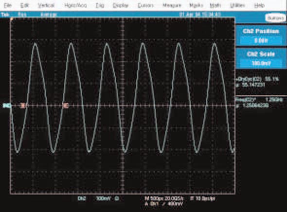
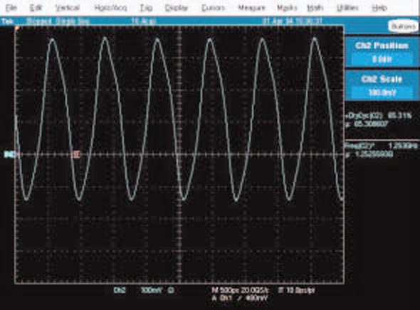
The NCP565-D voltage reference, using a reference voltage, VREF, of 0.9 V, creates a stable, controllable current source. The buffer inside the reference drives the bias voltage of an npn transistor and changes it until the voltage at ADJUST is equal to VREF. The current pulled through the transistor and the VN input is equal to VREF/R. R is the resistance between the emitter of the transistor and ground. Changing R changes this current, the voltage at VN, and, therefore, the duty cycle for the signal that the CML input sees. The circuit was tested with a 1.25-GHz clock. Figure 3 shows the waveforms of the differential signal (VP –VN) at the CML input set at 55% (Figure 3a) and 65% (Figure 3b). The described circuit increases the duty cycle; if the duty cycle needs to decrease, you'd connect the single-ended signal to VN and the current source to VP.
|
|||||
| Figure 3. | This photo shows duty cycles of 55.1% (a) and 65.3% (b). | ||||