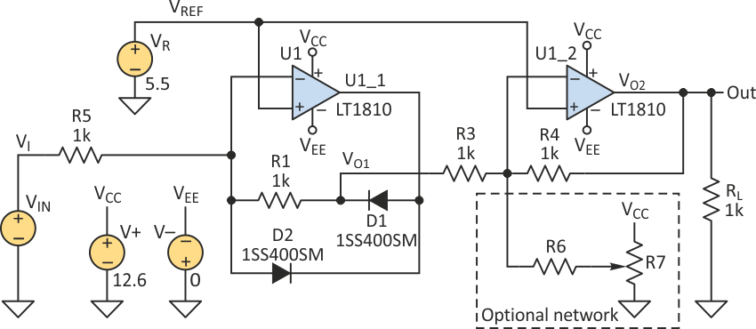
Limiter circuits are often needed to prevent a wide-range signal from overloading the next stage in the signal chain – this user-adjustable circuit provides bipolar limiting at precise preset value.
As the name implies, a limiter circuit (sometimes called a “clipper”) prevents a signal from exceeding desired thresholds, which would otherwise cause saturation and overload of the following stage. The circuit in Figure 1 precisely limits the wideband input signal Vi at the VREF level and can be used with both single and dual power supplies.
 |
||
| Figure 1. | This analog circuit, based on the LT1810 op amp, precisely limits input signal VI at reference level VREF. |
|
Output signal VO1 of the first stage, U1_1 (one-half of an LT1810, a dual 180-MHz, 350-V/µs low-distortion op amp), is precisely limited at the level of VREF , but with inverse polarity compared with the input signal. U1_1 has a gain of ‒1 for the input signal Vi, and a gain of +2 for the reference signal VREF.
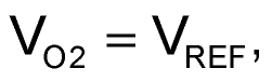
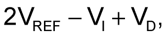
Since the positive input of U1_1 is referenced to VREF, the output signal is referenced to 2×VREF. Thus, while the input signal rises from zero to VREF, the output signal of the first stage decreases from 2×VREF to VREF. The second stage of limiter U_2 is an inverting amplifier with the gain of ‒1. It’s referenced to the VREF as well, and restores the original dc level and polarity of the input signal.
For the output of the first stage,
if VI ≤ VREF and
if VI ≥ VREF, while the output signal of the second stage is
if VI ≤ VREF, and
if VI ≥ VREF. (Note that the output-dc level, along with the limiting point, may be shifted by an optional network of R6 and R7; otherwise, that network isn’t used.)
D1 is a part of the negative feedback of U1_1, making it an "ideal diode" – as soon as VI reaches the VREF level, U1’s output voltage increases until it compensates for voltage drop VD of the diode. When VI is less than VREF and D1 is turned off, diode D2 is on and sends the output current of U1 directly to its input. This prevents U1 from negative saturation, which would significantly decrease the switching speed of the first stage.
The voltage level on the output pin of U1_1 is
and it reaches its maximum level with the minimum level of the input signal. This determines the maximum possible level of VREF, which doesn’t cause the distortion of the limiter's output signal at its minimum level of
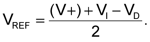
Here, V+ is the maximum output voltage of op amp at the chosen VCC, which is almost equivalent to VCC for the rail-to-rail op amp.
For the same reason, the minimum level of VREF should not be lower than VD; however, the input signal may significantly exceed VREF.
|
||||||
| Figure 2. | The LTspice simulation shows the limiter's response for a 1-MHz sine-wave signal (a) and a 2-µs piecewise-linear signal (b). |
|||||
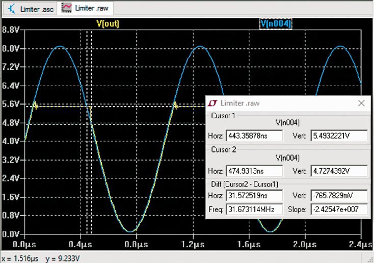
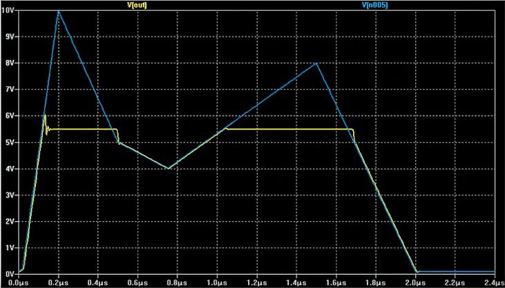
The LTspice simulation shows the limiter's responses for a 1-MHz sine-wave signal with 8-V peak-to-peak amplitude (Fig. 2a), and for a 10-V, 2-µs piecewise linear (PWL) signal crossing the limitation level several times (Fig. 2b), both with VREF of 5.5 V. The limiter is quite accurate within the entire output-voltage range of the op amp. The simulation demonstrates that limitation errors don’t exceed 8 mV and output setting time is within 30 ns around the limitation point. When compared to the "simple op amp clipper" of Ref. 1, this limiter works at much-higher frequencies and with significantly lower distortion.