Goh Ban Hok
EDN
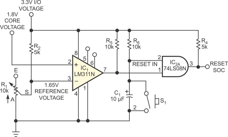
An SOC (system on chip) normally requires two power supplies – one for the core supply and the other for the I/O. To properly power up the chip, you need to get one of the power supplies ready before the other, according to the SOC's power-sequence requirement. Normally, the core voltage must power up first, and the I/O voltage powers up second. Instead of direct control of the power supplies, you can control the system reset to achieve a similar goal. Figure 1 shows the reset-conditioning circuit that can accomplish this task. In this circuit, the core voltage is 1.8 V, and the I/O voltage is 3.3 V. The reset-SOC signal produces a logic high when the core voltage gets ready before the I/O voltage. When the I/O voltage powers up first, the reset signal resets the SOC chip only after the core voltage powers up.
 |
||
| Figure 1. | This circuit for reset conditioning uses a comparator and an AND gate. | |
Comparator IC1 monitors both voltages. It operates on the 3.3 V I/O-supply voltage. Resistor R2 and variable resistor R1 form a voltage divider that lets you set the required voltage based on the core voltage. In this case, the reference voltage is 1.65 V at Pin 3. Pushbutton switch S1 provides a hard reset of the SOC.
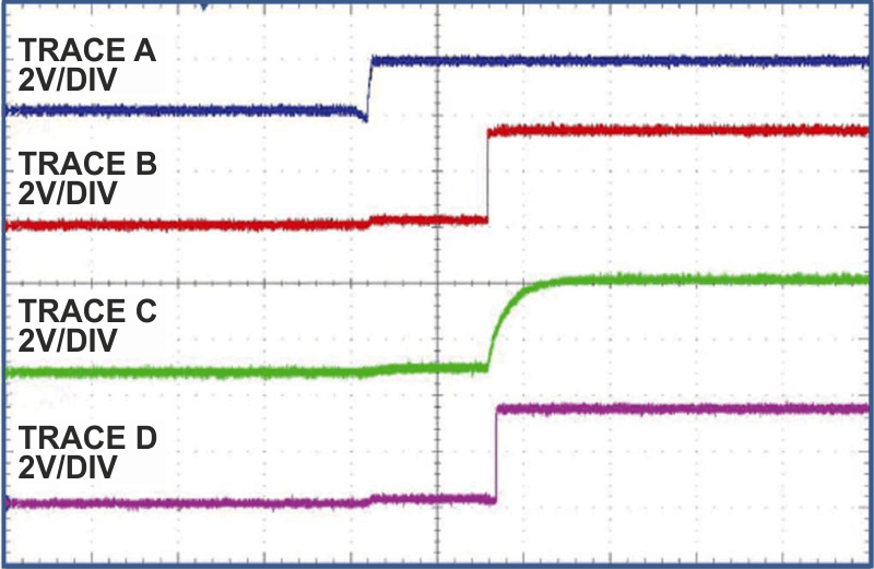
In Figure 2, the core voltage (Trace A) powers up first, and the I/O voltage (Trace B) follows. Comparator IC1 remains inactive until the I/O voltage activates. When the I/O voltage turns on, comparator IC1 and AND gate IC2A operate. As the voltage at IC1's Pin 2 is higher than that of Pin 3, the comparator produces a high at Pin 7, which pulls up through R5.
 |
||
| Figure 2. | When the core voltage (Trace A) powers up before the I/O voltage (Trace B), the reset signal (Trace D) waits for the capacitor to charge. |
|
The reset signal at IC2A's Pin 1 (Trace C) initially remains at zero and starts to charge capacitor C1 to the I/O voltage through R6. Depending on your application, you can adjust the RC time constant to suit your needs. The reset-in signal goes high after C1 charges to the logic-high level, which produces a logic-high signal at Pin 3 (Trace D), resetting the SOC.
 |
||
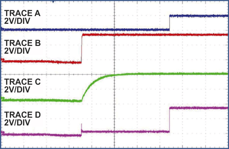
| Figure 3. | When the core voltage (Trace A) is late, the reset-SOC signal (Trace D) remains low. |
|
In Figure 3, the I/O voltage (Trace B) powers up first, and the core voltage (Trace A) follows. The core voltage powers up after the R6/C1 time constant. When the core voltage is 0 V, the comparator voltage at Pin 3 is higher than it is at Pin 2. Thus, the comparator produces a logic low at Pin 7. Pin 1 of AND gate IC2A remains high after the I/O voltage charges capacitor C1. The reset-out signal remains at zero state because the core voltage is not yet present. When the core voltage comes up, the voltage at comparator IC1's Pin 2 is higher than that of the threshold voltage at Pin 3. Thus, the comparator output's Pin 7 goes high. As reset remains high, the reset SOC of AND gate IC2 goes high after a propagation delay. This action resets the SOC.
 |
||
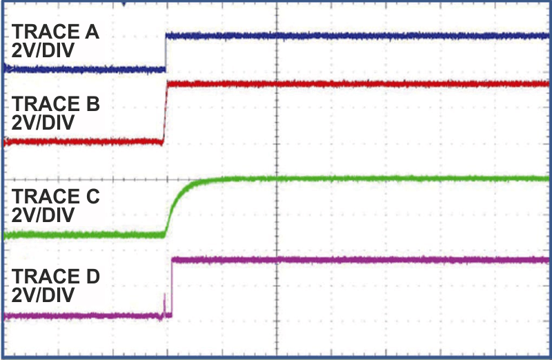
| Figure 4. | The reset signal (Trace D) goes high after both voltages come up and the capacitor charges. |
|
In Figure 4, the I/O voltage (Trace B) powers on first, and the core voltage (Trace A) follows. This case is similar to that in Figure 3 except that the core voltage powers up faster than the R6/C1 time constant. The comparator's IC1 output, Pin 7, goes high when the core voltage turns on, and the voltage at Pin 2 crosses the threshold of 1.65 V that resistor divider R1/R2 sets. However, the output reset's SOC signal goes high only when capacitor C1 charges to the logic-high level. AND gate IC2A then produces a high signal to reset the SOC.