Energy meters, heating/ventilation/air-conditioning (HVAC) systems, and high-power equipments that run on three-phase ac inputs pose a challenge to power-supply designers because nominal input voltage can be as high as 540 V ac. The challenge increases if the power supply must operate from 100 to 540 V ac. Design choices are numerous, and final system costs can vary dramatically with those choices. An abundance of parts is available for power supplies with input power as high as 240 V ac. High-voltage input-power supplies are, however, still a niche area for most semiconductor companies.
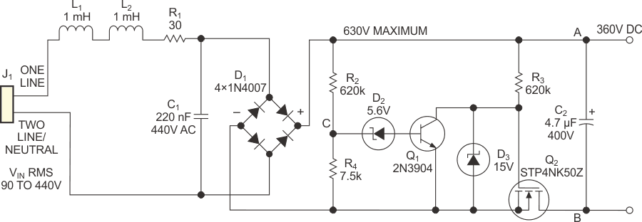
The power-supply circuit in the Figure 1 uses an input-chopper circuit that allows the clamping of input voltage to the flyback power stage so that the power is less than 400 V. That voltage lets you use a standard design technique for the flyback stage. The input chopper provides many advantages over prevailing high-voltage-input power supplies.
 |
|
| Figure 1. | A chopper circuit reduces power-bus voltage to less than 400 V dc per pin. |
Unlike a standard flyback converter, this circuit eliminates the need for a high-voltage MOSFET for the switch, thereby letting you use lower-cost, commonly available MOSFETs. Moreover, overall switching losses in the power supply decrease dramatically with the reduction in bus voltage. The circuit can use smaller and lower-cost transformers because of a reduction in creepage-clearance requirements.
This circuit's reduced bus voltage eliminates the stacked-FET-flyback topology and the need for two or more high-voltage capacitors. It also improves the overall efficiency of the system by eliminating the high losses of a stacked FET, replacing them with small losses from a bypass switch.
The 500 V, 2.7 Ω STP4NK50Z N-channel MOSFET switches at the line frequency. It turns on at a predetermined voltage, and it turns off at any higher voltage. It limits the voltage on C2 to approximately 360 V dc. When the voltage at the divider of R2 and R4 reaches approximately 6.3 V, or 360 V at the top of the divider, Q1 turns on and steals current from the gate of Q2, and the MOSFET turns off. The divider sets the level at which Q2 switches. All resistors are 0.25 W except for R1, which can be 2 W to survive surge. The circuit underwent testing with 12 W of output power at 90 to 440 V-ac input. The maximum input current to the power supply depends on the thermal performance of Q2.
