Second test circuit
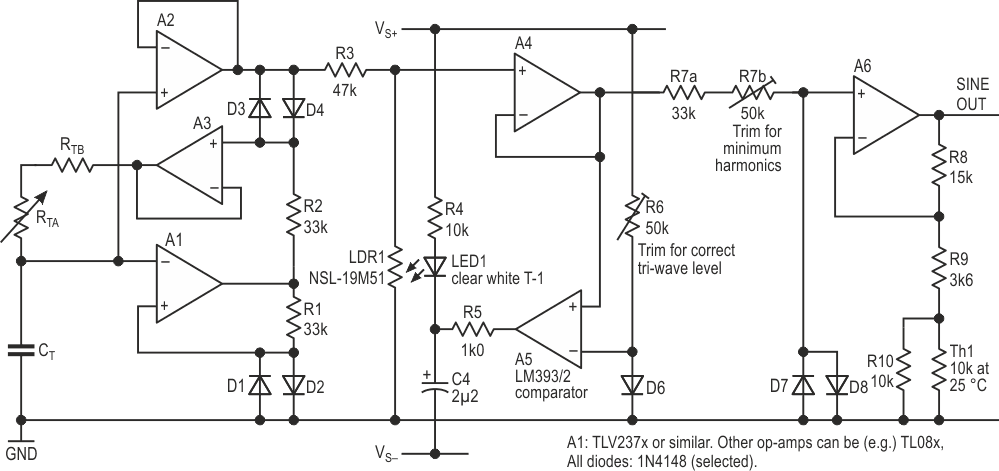
I looked at several types of AGC circuits (strictly, Automatic Level Control). JFETs are the usual starting-point but are inherently non-linear and need to be surrounded by lots of stuff to limit the signal voltage across them and cancel their remaining distortion – several op-amps and a couple of trimmers to do it properly. An LDR avoided the linearity problem, and while this solution may look almost barbarically simple, it works well here. Figure 4 shows the new circuit with the latest modifications.
 |
|
| Figure 4. | New tri-wave generator and sine converter test circuit, with AGC. |
A5, half of an LM393 dual comparator, senses when the tri-wave’s tip exceeds the reference value and then drives LED1 to illuminate LDR1, whose resistance falls, reducing the signal across R3. The reference is provided by R6 and D6, which track R1 and D2 in the oscillator itself. A4 buffers the output, which is now almost constant below 10 kHz and only 10% up at 25 kHz. (LDR1 was a Silonex NSL-19M51, the LED being a generic T-1 clear white 8 cd device, though an efficient 550 nm green/cyan one would match the LDR’s response better. Thick, black heat-shrink joined and shielded them.) An op-amp with a series pull-down diode replacing R5 also works, but only up to 10 kHz or so owing to its slower response.
At very low frequencies, the overshoot is minimal, so the LED is barely tickling the LDR when using the oscillator of Figure 2. With a higher input from that or another source – beyond 10 V pk-pk on test – the tri-wave level is still defined by VF: the AGC is just working harder. It is best to pot high levels down first, though.
We now have two options for faking a sine: one where we start with a level defined by the oscillator itself, and another where the level is arbitrary.
Whatever the source, we now have a tri-wave whose amplitude is defined by D6’s VF but is that really the optimum level?
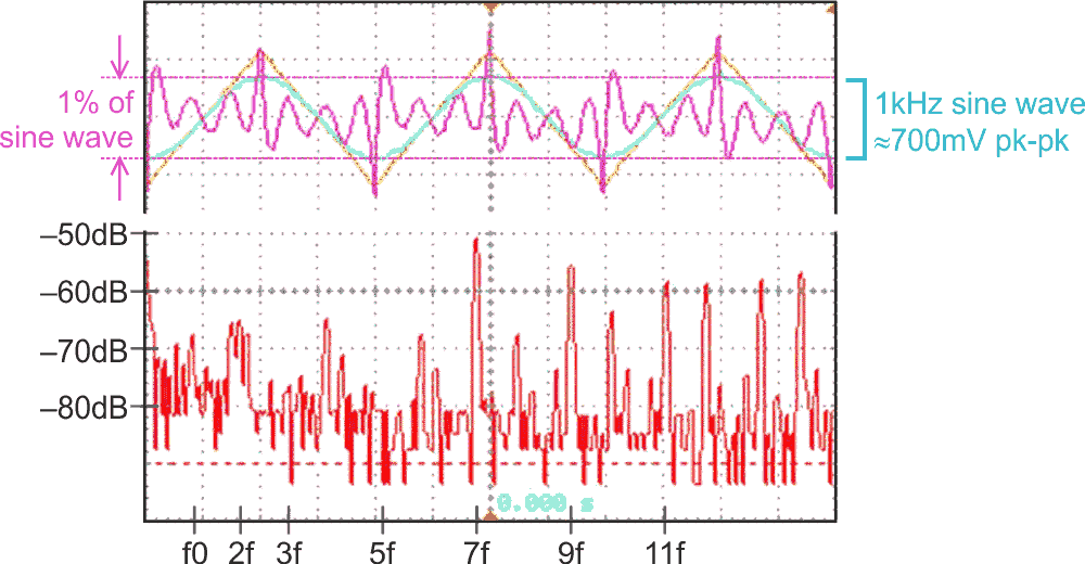
Intuitively, that would seem to be the same as the squashing diodes’ VF, assuming the series resistor to be ideal, and so it proved – with a pleasant and almost shocking surprise in store. With R6 and R7 finely adjusted, the third and fifth harmonics completely disappeared! Figure 5, explained below, shows this.
 |
|
| Figure 5. | Results from Figure 4’s circuit. The top shows the original triangle and the resulting sine, with harmonics at 100 times their scale; the bottom shows their FFT. |
But with the slightest mismatch anywhere, one or both harmonics came back. The tri-wave’s level needed to be millivolt-accurate, and A5’s input offset meant that R6 had to be adjustable. The best and most consistent results came when R6 was replaced by a precision current source (not shown) delivering ~275 µA into D6, which eliminated second-order power supply effects. (That’s a higher current than expected because of the offset.) The critical value of R7 was remarkably close to R1/R2 – close to 33k – so perhaps, with perfect components and no AGC necessary, R1, R2, R6, and R7 would all be identical, and with a critical value close to 30k. I leave this one for the theorists!
Removing the fundamental with the notch filter showed that the seventh and higher harmonics were now dominant and couldn’t be tuned out. (Kindly ignore the pesky, residual even ones.) The seventh was at around –50 dB, or 0.3%; after that, the higher, the lower. Figure 5 is a composite of traces: at the top is the original triangle and the resulting sine, with the distortion products – the harmonics – at 100 times their scale; below that, their FFT. This implies that the distortion limit is about 0.4-0.5% in total.
And the output level from the diodes? Intuition (and the waveforms’ geometries) said that the sine’s amplitude should be 1/√2 of the triangle’s, but now it’s wrong: all measurements homed in on 0.666… Presumably the residual harmonics account for the difference, though the numbers look wrong. I expect that a mathematician familiar with the various series defining sines, and how those relate to Fourier analysis, would find the answer obvious.
A6 buffers and amplifies the newly generated sine wave. Note that we have added Th1 – a standard 10k (at 25 °C) thermistor – in the gain-defining network. While the amplitude variation with temperature was unimportant in practical use, it seemed only right to compensate for it. According to LTspice, this network will give the gain we need to raise the sine wave’s amplitude to ~2.2 V pk-pk, or 0 dBu, from 0 to 50 °C. (And that’s the only bit of simulation used here. I hope their diode models are good.) Distortion still varies with temperature. Although D6 and D7/8 are matched in isolation, their drive currents are different, so their functioning VFs neither match nor quite track with temperature. Perhaps mixing another NTC thermistor in with R7 would cure this…
Care needs to be taken to minimize second-harmonic distortion, or waveform asymmetry. Power rails must be well-matched or second-order effects creep in, though apart from the AGC, the circuit is symmetrical and inherently well-balanced. The diodes must be carefully matched in pairs for forward voltage. (Taping a strip of ~50 1N4148s to a sheet of paper, measuring and annotating each one, and then selecting pairs, worked well, for this and other projects.) Surprisingly, dual diodes, or those that I have checked, don’t match internally very well. Offsets within the op-amps cause slight asymmetry. I trimmed most of it out by connecting a 100k pot across the supplies with a 10M resistor from its slider to the junction of R3 and LDR1 (not shown): crude, but effective, if a little sensitive to supply variations.
The harmonic content still rises with frequency, though much less than before, but in the real world, if the 3rd and the 5th are significantly lower than the 7th harmonic, we’re doing well. Above 3 kHz, distortion starts to rise, but the harmonics are gradually being pushed beyond the notional top of the audio band at 20 kHz. I estimate that ~1% THD (–40 dB) is reached by ~8 kHz, and ~3% (–30 dB) by 20 kHz. This circuit can run at way beyond 100 kHz, but can’t then be recommended for waveform purity! (By about 25 kHz, the tri-wave has turned into a pretty good sine, anyway.)
Calibration of a tuning scale at low frequencies will not be matched on higher ranges because of A1’s performance: the inherent delays affect the tuning law as well as the tri-wave’s amplitude. On my original build, I used a spare section of the range selector switch to vary RTB – the extra end resistance – which helped keep the ends of the scale within 5%.
Conclusion and discussion
Our quest is now at and end, and we have discovered several curious and useful things on the way. We have a novel oscillator which is inherently ideal for squashy sine wave generation, and we can precisely match other sources to that process. We have a better understanding of the limits to what is possible but have found some nice ways of optimizing the practical results. And there are still many unanswered questions, with much food for thought about the underlying math!
Our empirical conclusion: for optimum performance, the applied tri-wave must have exactly the amplitude that matches the VF the squashing diodes would have, if they were being driven in the same way as the reference for that tri-wave.
But the gold at the end of our rainbow is at best an alloy: our squashed triangle can never be a pure sine, for even when we have tamed the lowest harmonics, there will always be the small, sharp teeth of the upper ones to snap at us. By the time we have fixed all the other problems, we might as well have used all those devices in a “proper” sine-wave generator, using a two-integrator/bi-quad loop oscillator or even a Wien bridge, capable of much lower distortion and generally cleaner performance.
For a simple, reliable sine wave generator, good for level-checking and lining up if rubbish for distortion checking, this solution has proved excellent, while optimizing it was most instructive.
References
- Woodward. Stephen. “Dual RRIO op amp makes buffered and adjustable triangles and square waves.”
- Michael A. Shustov. “Rectangle and triangle waveform function generator.”
- “Diode modelling”
- Abell, Einar. “Linear ramp generator uses one op-amp.”