This design idea revisits another: “PWM power DAC incorporates an LM317” (Ref. 1). Like the earlier circuit, this one implements a power DAC by integrating an LM317 positive regulator into a mostly passive PWM topology. It exploits the built-in features of that time-proven Bob Pease masterpiece so that its output is proportional to the guaranteed 2% precision of the LM317 internal voltage reference and is inherently protected from overloading and overheating.
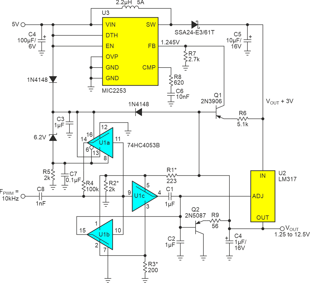
However, unlike the earlier design idea that requires a separate 15 V DC power input, this remake (shown in Figure 1) adds a switching input boost preregulator so it can run from a 5 V logic rail. The previous linear design also has a limited power efficiency that actually drops below single-digit percentages when driving low voltage loads. The preregulator fixes that by tracking the input-output voltage differential across the LM317 and maintains a constant 3 V. This is the just adequate dropout-suppressing headroom for the LM317, minimizing wasted power.
 |
|
| Figure 1. | LM317 and HC4053 combine to make a PWM power DAC while Q1 forces preregulator U3 to track and maintain a constant 3 V U2 I/O headroom differential to improve efficiency. |
As described in the earlier DI (Ref. 1), switches U1b and U1c accept a 10-kHz PWM signal to generate a 0 V to 11.25 V “ADJ” control signal for the U2 regulator via feedback networks R1, R2, and R3. The incoming PWM signal is AC coupled so that U1 can “float” on U2’s output. U1c provides a balanced inverse of the PWM signal, implementing active ripple cancellation as described in “Cancel PWM DAC ripple with analog subtraction” (Ref. 2)
Note that R1||R2 = R3 to optimize ripple subtraction and DAC accuracy. This feedback arrangement makes U2’s output voltage follow this function of PWM duty factor (D):
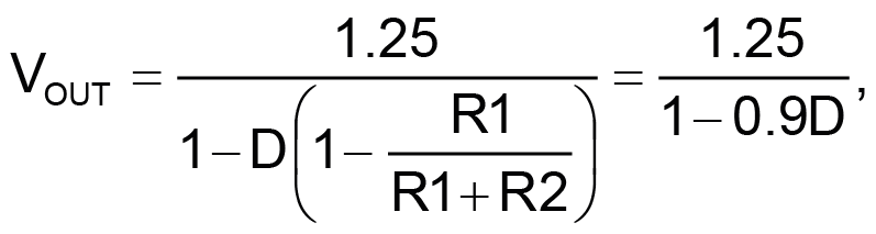
as graphed in Figure 2.
 |
|
| Figure 2. | VOUT (1.25 V to 12.5 V) versus PWM D (0 to 1) where VOUT = 1.25 / (1 – 0.9 D). |
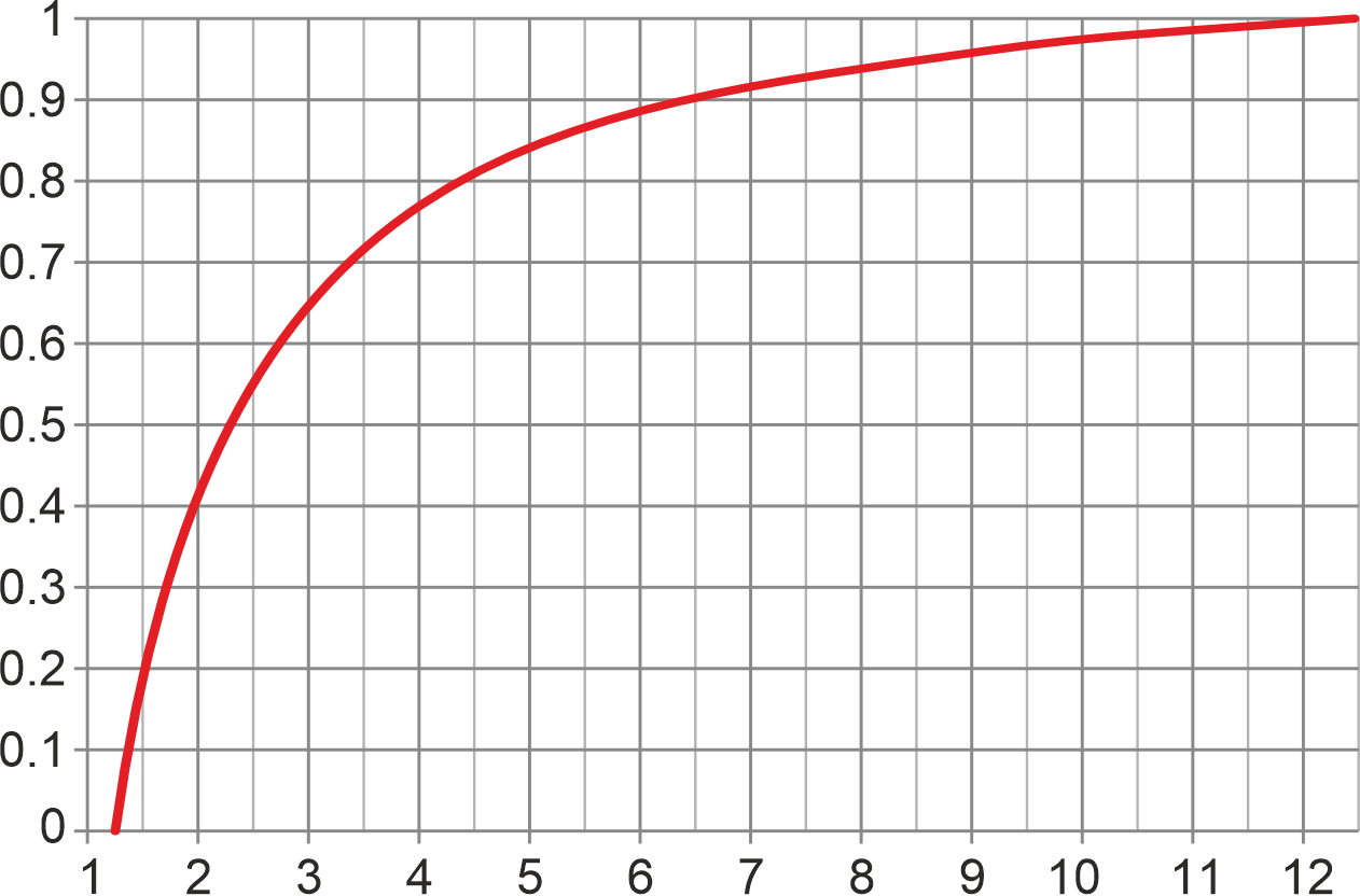
Figure 3 plots the inverse of Figure 2, yielding the PWM D required for any given VOUT.
 |
|
| Figure 3. | The inverse of Figure 2 or, the PWM D required for any given VOUT, where PWM D = (1.111 – 1.389/VOUT). |
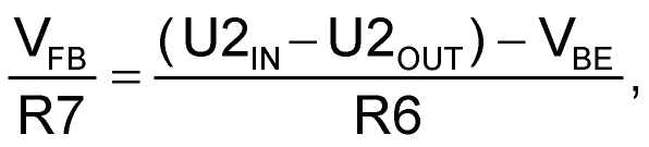
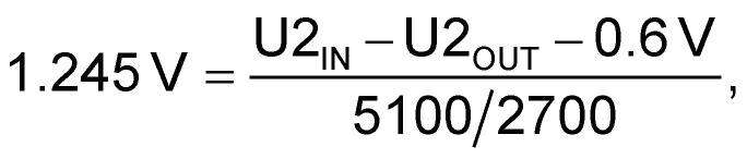
About that tracking preregulator thing: Control of U3 to maintain the 3 V of headroom required to hold U2 safe from dropout relies on Q1 acting as a simple (but adequate) differential amplifier. Q1 drives U3’s VFB voltage feedback pin to maintain VFB = 1.245 V. Therefore (where VBE = Q1’s emitter-base bias):

Meanwhile, deducing what Q2 does is left as an exercise for the astute reader. Hint: It saves about a third of a wattage over the original DI at VOUT = 12 V.
Note, if you want to use this circuit with a different preregulator with a different VFB, just adjust:

References
- Woodward, Stephen. "PWM power DAC incorporates an LM317."
- Woodward, Stephen. "Cancel PWM DAC ripple with analog subtraction."
