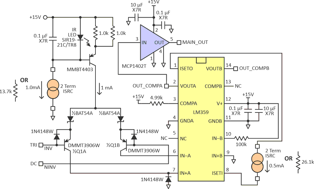
Dual precision comparators are needed in many designs, such as for industrial and instrumentation applications, to generate accurate pulse-width modulated (PWM) waveforms with very high (>99%) and very low (<1%) duty-cycle percentages. This design idea (Fig. 1) improves on designs based on the common LM311 and LT1011 devices, both of which require resistor pull-ups and have asymmetric timing paths. The features of this new design include matched, short propagation delays (TPD); accurate duty-cycle generation; push-pull, rail-to-rail output; and operation from a supply above 15 V.
 |
|
| Figure 1. | The schematic and text include several circuit options (current source, transistor bias). |
The circuit is based on the LM359 high-speed video op amp with an additional bipolar PNP input stage, and an MCP1402T output driver powered with a single +15-V supply. The LM359 is used to get a high-speed “IC Process” device to meet a comparator’s specifications. This IC also permits design changes at a low level because it has both input and output programming-current pins, and the compensation node is available as well. Input and output programming currents are driven by a 0.5-mA source.
Since this op amp is a dual device, one half is connected as a comparator and the other half remains as a spare. A spare is shown to define its connections. A transconductance stage is placed ahead of the LM359’s current-mode input to enable a voltage-mode input. The gain is reduced at the cascade stage’s high-impedance node (COMPA pin) by the 4.99-kΩ resistor. A capacitor in parallel with the resistor also controls the bandwidth of the LM359. The IN– terminal of the LM359 is an additional high-impedance node and it, too, can be locally compensated to GND. (Figure 43 of the LM359 datasheet, "Adding a JFET Input Stage," helped spark ideas for the input stage.)
The output of the LM359 is connected to the input of the MCP1402T, a device that can drive rail-to-rail and drive capacitive loads very well. The LM359’s supply voltage can even be set to a lower voltage level and the MCP1402T can still be set to drive to a 15-V output level. The maximum supply voltage of the comparator is limited by the MCP1402T to 20 V dc, which means that is can be used for 18-V designs.
Using a higher supply voltage improves signal-to-noise ratio (SNR), as there is a larger signal for a given amount of noise. Also, large input signals dominate any voltage-offset terms, which is an advantage of using the higher voltage supply. (Note that the output polarity can also be easily changed on a fabricated printed-circuit board by using a MCP1401T in place of the MCP1402T.)
The circuit uses both 1-mA and 0.5-mA (two-terminal) current sources. In the original design, custom sources were used, but resistors can be used in their place (although with a reduction in supply rejection performance). An LM334 is also an option, as well as a JFET with a source resistor to control VGS. The 1-mA current biases the SIR19-21C/TR8 IR LED; a 1.2-V shunt voltage reference can be used in place of the IR LED. The 1N4148W diodes at the transconductance input stage protect against reverse-biasing at the emitter-base junctions, while the BAT54A prevents current from one side or the other of the differential pair adding to the tail current.
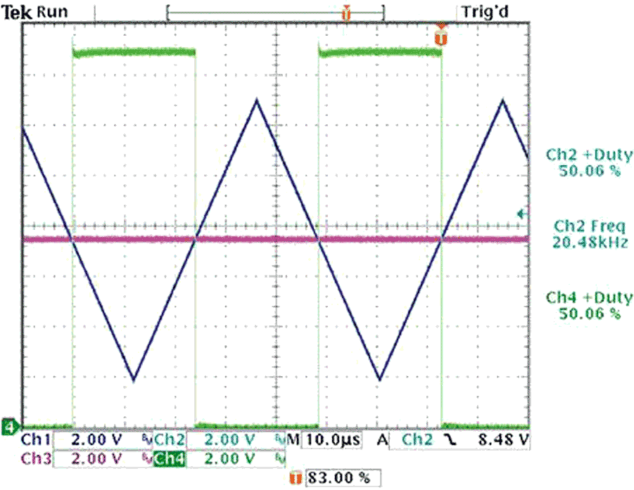
The Figure 2 shows measurements of key nodes in the comparator and the matching of both comparators. The measured propagation-delay mismatch causes the 0.06% offset from 50% duty cycle.
 |
|
| Figure 2. | CH1 (dark blue) is the triangle to the input stage’s inverting terminal; CH2 (light blue) and CH4 (green) (on top of each other) are the square- wave outputs of the MCP1402Ts; and CH3 (pink) is the half-supply dc-voltage level to the input stage’s non-inverting terminal. |