Martin Murnane, Analog Devices
Solar Photovoltaic Inverters
A major portion of the electrical energy produced directly from the sun’s radiation is generated by solar photovoltaic (PV) cells, which convert photons of light energy to electron flow that constitutes an electrical current. Figure 1 shows an aerial photo of a large solar PV installation.
 |
|
| Figure 1. | Solar PV installation, Yuma County, Arizona. |
A solar photovoltaic (PV) inverter converts electrical power from a solar panel and deploys it to the utility grid efficiently. DC power from the solar panels, which act like a dc current source, is converted to ac and fed onto the utility’s grid in the correct phase relationship – with up to 98% efficiency. The PV inverter conversion process can occur in one or more stages.
Stage 1 is typically a dc-to-dc conversion from the low voltage-high current solar cells that constitute the panels, to the high voltage-low current levels compatible with the ac voltage of the grid. This stage may not be necessary, depending on the topology and if enough solar cells are connected in series, on the dc side, to ensure a stable high voltage under all load conditions.
In Stage 2, dc is converted to ac, typically using an H-bridge topology. PV inverter designs may use variations of the H-bridge, such as neutral-point clamping (NPC), to improve efficiency and reduce reactive power in the system.
Early solar PV inverters were simply modules that dumped power onto the utility grid. Newer designs emphasize safety, intelligent grid integration, and cost reduction. Designers are looking to new technology, not used in existing solar inverter modules, to improve performance and reduce cost.
A key element is computer-based instrumentation and control, but an isolation barrier must protect measurement and computation circuitry from the power-handling circuitry – as well as from transient signals due to switching. This article will suggest how iCoupler® isolation technology can reduce cost, increase smart grid integration, and improve safety of solar PV inverters by using Analog Devices isolated analog-to-digital converters (ADCs) and gate drivers.
Smart Grid
What is a smart grid? IMS Research defines a smart grid as “a utility supply infrastructure with the inherent ability to match and manage generation and consumption efficiently, while obtaining maximum benefits from the available resources.” This means that the new generation of solar PV inverters requires more intelligence to connect with the smart grid, especially to deal with the imbalance on occasions when more power is available from multiple sources than is needed by the grid. For this reason, the focus of PV system intelligence needs to be on grid integration, where each contributor to the system power must cooperate to stabilize the grid, rather than simply supplying power open-loop. Grid integration requires better measurement, control, and analysis of the quality of the energy fed to the grid. In addition, new directives and higher technical requirements call for new technology.
An important local feature of smart grid integration may, therefore, be energy storage to reduce turbulence on the grid by storing unneeded electrical energy until it is needed during peak usage. The rest of this article will focus on the role of electrical isolation in protecting the instrumentation circuitry used to measure and control the sources, interconnections, and storage elements – with primary emphasis on the key role of iCoupler technology. The AD7401A isolated ADC and the ADuM4223 isolated gate driver, in particular, offer performance that will meet the demands of new solar PV inverter designs.
Isolation Technology
In iCoupler technology, transformers couple data between two separately powered circuits while avoiding any galvanic connection between them. The transformers are fabricated directly on chip using wafer-level processing. A high breakdown polyimide layer underneath the gold layer insulates the upper coil from the lower one. Input logic transitions, encoded using 1 ns pulses, are routed to the transformer’s primary side. The pulses, coupled from one transformer coil to the other, are detected by the circuitry on the secondary side of the transformer.
Isolated ADC
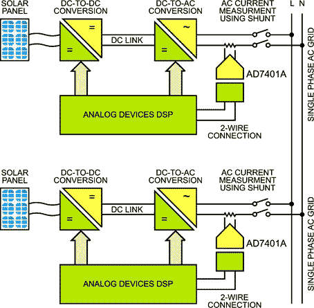
Figure 2 shows a pair of solar PV inverters like those described in the introduction. Tied to a power bus that is connected to the grid, they are independently measured and switched. Each solar panel is connected to its dc-to-dc step-up circuit, then to a dc-to-ac inverter. (When used, a storage battery would be connected and switched, under control. Any discussion of storage is omitted to simplify this explanation).
 |
|
| Figure 2. | Solar PV system example. |
A digital signal processor (DSP) controls the process. The AD7401A isolated ADC measures ac output current of the order of 25 A. Solar PV inverter systems may or may not have an isolation transformer at the output. If the transformer is omitted to save cost, the solar PV inverter must also measure any dc component of the output current. The presence and magnitude of this “dc injection” is a critical matter, as too much dc current injected onto the grid may saturate any transformers in its path. This value must be limited to the low milliampere range, so the AD7401A must measure both ac current in the 25-A range and low-millliampere dc.
 |
|
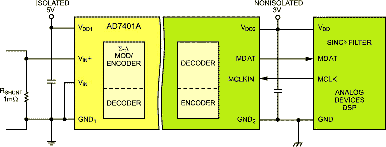
| Figure 3. | Isolated AD7401A ADC. |
The AD7401A iCoupler – isolated Σ-∆-modulator ADC, continuously samples the voltage across the current shunt, as shown in Figure 3. Its output is a 1-bit data stream, which is isolated and fed directly into a DSP. The density of ones in the output stream represents the input amplitude, which can be reconstructed with a digital filter implemented in the DSP.
Isolation is required within solar PV inverter systems, primarily because of the high voltages appearing on an ac grid. The ac voltage, even in single-phase systems, can peak at 380 V. The AD7401A’s isolation can handle bipolar voltage up to 561 V, which makes it highly suitable for this application. A key advantage to using the AD7401A is that its small package allows the ADC to be located very close to the actual ac current shunt, whereas the DSP may be some distance away – or even on another board in the system. This improves the accuracy and reliability of data in the measurement and control system. The ADC output data is sent to the DSP serially via a single-bit stream at a 16-MHz clock rate, supplied by the DSP.
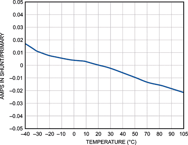
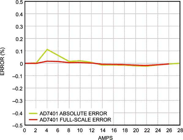
This system can measure ac currents up to 25 A and dc injection in the low milliampere range. Figure 4 illustrates offset and linearity errors of the AD7401A SMS solar module. This shows the offset current in the shunt at ±20 mA over temperature. Thus, the module can measure dc injection down to 20 mA, as well as 25-A (or greater) system currents using a single solution. Current transformers and other types of measurement systems might require two devices, one for large ac currents (25-A range) and one for small dc currents (300-mA range). This is one example of how iCoupler technology can provide smart grid integration with cost savings.
 |
 |
||
| (a) | (b) | ||
|
Figure 4. Offset and linearity of the AD7401A SMS solar module. a. Offset vs. temperature. |
|||
To minimize power loss (and thermal errors due to self-heating) in the shunt, its resistance needs to be kept to as low a value as possible, at typically 1 mΩ. The very high resolution of Σ-∆ converters allows current shunt losses to be kept on par with traditional magnetic transducer solutions while achieving better accuracy and lower offset, as shown in Figure 4.
Although full-scale accuracy is extremely good, the real test of a device’s linearity is its absolute error, especially at low ranges. Absolute error is the error associated with the measurement over its range of values, as opposed to simply the error at full scale. Some current transformers specify their devices as 0.1% full-scale range. While this looks good, it may not tell the full story.
From the data shown in Figure 4, the absolute error of current measurement using the AD7401A is quite low over the entire range, indicating low nonlinearity and reduced harmonic distortion of the waveform from the output of the solar PV inverter. This, in turn, helps reduce harmonic distortion when integrated with the grid, providing another example of how this new technology improves performance.
Isolated Gate Driver
The higher a solar PV inverter’s efficiency, the more energy it can generate per year from a given solar input, which leads to a better return on investment for a solar farm. Due to their lower cost, the current trend is toward having transformerless electrical systems feed into the public utility grid. The correspondingly higher levels of efficiency in the inverter come with a need for more attention to internal isolation of its measurement and control electronics, that is, the isolation required between the power section of the inverter’s MOSFET and/or gate drivers and the lower voltage circuitry.
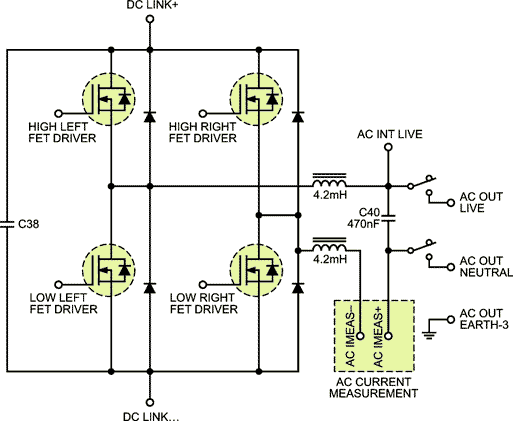
Figure 5 shows one possible implementation of an H-bridge configuration for the dc-to-ac converter of a typical solar PV inverter. The dc link voltage in the circuit can range from 300 V up to 1000 V for the new SiC type JFETS on the market today. The current output waveform of the H-bridge is filtered using inductors and capacitors. Output relays connect the filtered output to the grid in a controlled manner. A gate driver is required to drive the gate and source terminals of the MOSFETs in a high-voltage environment – one more occasion for isolation in solar PV inverters.
 |
|
| Figure 5. | H-bridge circuit example for solar PV inverter. |
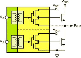
As an example, the ADuM4223 4-A isolated, dual-channel gate driver with two independent isolation channels is shown in Figure 6. It has a maximum propagation delay of 60 ns and a common-mode transient immunity of >100 kV/μs (max). This device meets various standards, such as the relevant sections of DIN VDE0110, DIN VDE 088410, and UL1577, as described in the data sheet.
 |
|
| Figure 6. | ADuM4223 gate driver. |
The following are some of the most important isolation parameters of the ADuM4223:
- Maximum continuous working voltage
- AC unipolar and dc 1131 V
- AC bipolar 565 V
- Surge isolation voltage 6 kV
- Rated dielectric insulation voltage 5 kV.
The device has two channels in one package, one each for the high-side and low-side MOSFETs. Having both channels in one package saves both cost and space on a PCB.
With conventional optocouplers, either a single optocoupler with level shifting on the isolated gate is required, or two optocouplers may be needed (see the MS-2318 technical article for further details) – another example of how this new isolation technology can reduce cost.
Another important issue for solar PV inverters is the high common-mode transient immunity required to ensure that any large transients (dV/dt) in the system do not cross the isolation barriers, whether coupled capacitively or otherwise, as this would make it possible for both high-side and low-side MOSFETs to turn on simultaneously (and catastrophically). The ADuM4223 has a high common-mode transient immunity: >100 kV/μs (max), providing yet another example of how this new technology can improve safety in the system.
Conclusion
Galvanic isolation is an important requirement for the measurement and control systems needed to implement smart grids that integrate large numbers of solar photovoltaic inverters. Analog Devices isolated ADCs, with their ability to measure both large currents and dc injection currents in a single solution, can contribute compactly and efficiently to smart grid integration circuitry. ADI isolated gate drivers, with good common-mode transient immunity specifications, contribute to safety and reliability of these new PV inverter systems.
New technology will be a major factor contributing to smart grid integration and the safe and efficient production of green energy – with key roles in grid stabilization and improved safety for all personnel working on grid systems. The isolation products discussed here are salient examples of innovations available from the broad Analog Devices portfolio of products for industrial measurement and control – for both current and future designs.
