Alan Walsh, Analog Devices
EDN
A common issue that arises when designing an ADC circuit is how to protect the ADC inputs from over voltage. Protection of ADC inputs have many scenarios and potential solutions. ADCs from all vendors have similar needs in this respect. This article gives an insight into what issues can arise in the case of overvoltage, how they occur and potential remedies.
Over drive of ADC inputs generally occurs when the rails of the driving amplifier are significantly greater than the max input range of the ADC e.g. amplifier runs from ±15 V and ADC input is 0-5 V. This is particularly common in industrial designs where high voltage rails are used to accept ±10 V inputs and also power signal conditioning/driver stages prior to the ADC e.g. PLC modules. If a fault condition occurs such that the driving amplifier rails it can cause damage to the ADC by exceeding its max rating or disturb simultaneous/subsequent conversions in a multi ADC system. This article will focus on how to protect a precision SAR ADC like the AD798X family but can be applied to other ADC types.
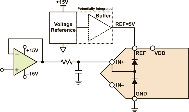
Let’s consider the scenario below in Figure 1.
 |
|
| Figure 1. | Typical ADC circuit in the PulSAR family of ADCs. |
This circuit is representative of what we see in the AD798X (e.g. AD7980) family of PulSAR ADCs. There are protection diodes between the input, the reference and ground. These diodes are capable of handling high currents up to 130 mA in the case of the AD798X family but only for a few milliseconds, not for longer periods or repeated overvoltage. On some products like the AD768X/9X (e.g. AD7685, AD7691) family of parts the protection diodes are to the VDD pin instead of REF. On these parts the VDD voltage is always greater than or equal to REF. Generally this works better as VDD is a stiffer rail for clamping and is not as sensitive to disturbance.
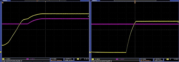
In Figure 1 if the amplifier was to rail towards the +15 V rail then the protection diode to REF will turn on and the amplifier will try to drag the REF node up. If the REF node is not driven by a strong driver circuit then the voltage at the REF node (and input) will rise above the absolute maximum rated voltage and the ADC may be damaged if the voltage exceeds the breakdown voltage of devices on that process. See Figure 3 below for an example of the ADC driver railing towards +8 V overdriving the reference voltage (5 V). Many precision references have no sink current capability which is a problem in this scenario. Alternatively the reference drive circuit may be strong enough to hold the reference close to its nominal value but will still be disturbed from its precise value.
 |
|
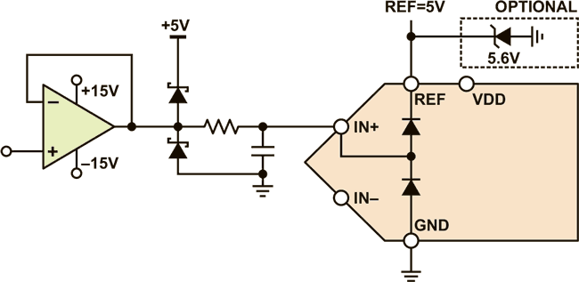
| Figure 2. | Clamping the output of the amplifier to protect the ADC input. |
In a simultaneous sampling multi ADC system sharing the one reference, this means the conversions on the other ADCs will be inaccurate as the system depends on a highly accurate reference voltage. Subsequent conversions may also be inaccurate if the recovery time from the fault condition is long.
There are a few different approaches or ones used in combination to mitigate this issue. The most common is to use schottky diodes (e.g. BAT54 series) to clamp the output of the amplifier to the range of the ADC. See Figures 2 and 3 for an illustration. It may also be possible to use diodes to clamp the input to the amplifier if it suits the application needs.
 |
|
| Figure 3. | Yellow = ADC input, Purple = Reference. Left – without schottky diodes. Right – with schottky diodes. |
In this case the schottky diodes are chosen for their low forward voltage drop such that they turn on before the internal protection diodes in the ADC. The series resistor after the schottky diodes also helps limit the current into the ADC if the internal diodes turn on slightly. For extra protection, if the reference has little/no sink current capability, a zener diode or clamp circuit could be used on the reference node to guarantee the reference voltage cannot be pulled too high. In the above example a 5.6 V zener is used for a 5 V reference.
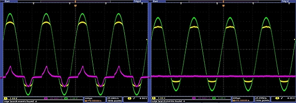
An example is shown in Figure 4 of the effect on the reference input (5 V) of adding schottky diodes to the ADC input when overdriving the ADC input with a sine wave. The schottky diodes are connected to ground and a 5 V system rail capable of sinking current. Without the schottky diodes there is a reference disturbance when the input exceeds the reference and ground by a diode drop. As can be seen the reference disturbance is completely removed with the schottkys.
 |
|
| Figure 4. | Yellow = ADC input, Green = ADC driver input, Purple = Reference (AC coupled). Left image without schottky diodes. Right image with schottky diodes (BAT54S) added. |
Attention needs to be paid to the reverse leakage current of the schottkys as this may introduce distortion/non-linearity during normal operation. This reverse leakage is very temperature dependent and is generally specified in the diode datasheet. A good option are the BAT54 series of schottky diodes (2 µA max at 25 °C, ~100 4 A @ 125 °C).
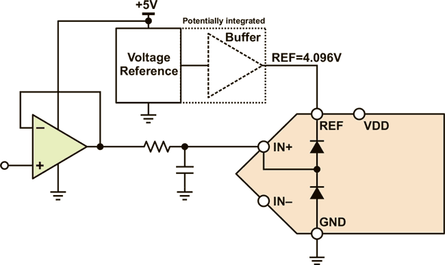
A way of eliminating over voltage issues completely is to use a single supply rail for the amplifier. This means the driving amplifier can never swing below ground or above the max input voltage if the same supply level is used as for the reference voltage (max input voltage), in this example 5 V. It may be possible to use the reference circuit to supply the amplifier directly if it has sufficient output current/ drive strength. Another possibility as shown below in Figure 5 is to use a slightly lower reference value (e.g. 4.096 V when using a 5 V rail) resulting in significantly reduced voltage overdrive capability.
 |
|
| Figure 5. | Using a lower reference value to reduce voltage overdrive capability. |
These approaches solve any issue with overdriving the input but the tradeoff will be limited input swing/range to the ADC because of amplifier headroom/footroom requirements. Typically a rail-to-rail output amplifier can get within 10’s of mVs of the rail but it is also important to consider input headroom requirement, which can be 1 V or more, as this will limit the swing further in a buffer/unity gain configuration. This approach offers the simplest solution in terms of no additional protection components needed but depends on having the correct supply voltage and possibly a rail-to-rail input output (RRIO) amplifier.
The series R in the RC filter between the amplifier and RC can also be used to limit the current seen at the ADC input during an overvoltage condition. However this will be a tradeoff between current limiting and ADC performance. Larger series R will give better input protection but result in greater distortion in the ADC performance. This may be an acceptable tradeoff especially if the input signal bandwidth is low or the ADC is not being run at the full throughput rate as more series R can be tolerated in this case. The size of R acceptable for the application can be determined experimentally.
As discussed above when protecting the ADC input there is no silver bullet solution but depending on the application requirements different individual or combined approaches may be taken to give the desired level of protection with corresponding performance tradeoffs.