Voltage reference ICs provide an accurate, temperature compensated voltage source for use in a variety of applications from A/D converters to medical devices
Voltage references are available with fixed and adjustable reference voltage outputs. Adjustable output is set by a resistor divider connected to a reference pin. These references are either shunt (two-terminal) or series (three-terminal) types. These ICs usually come in families of parts that provide specific accurate voltages. Some families can have up to six different values with output voltages from 1.225 V to 5.000 V and tolerances ranging from ±0.25% to ±2%. Initial output voltage accuracy and temperature coefficient are two of the more important characteristics.
Among the characteristics that an ideal voltage reference should have are:
- Output voltage independent of temperature changes
- Output voltage independent of load current
- Output voltage independent of time.
The ideal voltage reference should also have:
- Perfect initial accuracy
- Current source and sink capability
- Low quiescent current (or power dissipation)
- Low noise
- Reasonable cost
However, these ideal characteristics are unattainable, so the designer must consider the following:
Reference Sources include zener diode usually used in two-terminal shunt devices. A major advantage of zeners is the wide range of voltages that their wide range, from 2 V to 200 V. They also have a wide range of power handling capability, from several milliwatts to several watts. Disadvantages of zener diodes are that they may not be precise enough for high-precision applications. Also, their power consumption makes them a tough fit for low-power applications. Another concern with a zener reference source is the relatively high output impedance of some types.
Another reference source is the bandgap usually used in three-terminal series ICs. A bandgap voltage reference is a temperature independent voltage reference circuit widely used in integrated circuits, usually with an output voltage about 1.25 V, which is close to the theoretical 1.22 eV bandgap of silicon at 0 K.
Shunt references are similar to zener diodes in operation because both require an external resistor that determines the maximum current that can be supplied to the load. The external resistor also sets the minimum biasing current to maintain regulation. You should consider shunt references when the load is nearly constant with minimal power supply variations.
Series references do not require any external components and they should be considered when the load is variable and lower voltage overhead is important. They are also more immune to the power supply changes than shunt references.
Series references have some advantages over shunt types. Shunt references require a resistor that must be chosen to supply the maximum current demanded by the load. When the load is not operating at this maximum current, the shunt reference must always sink this current, resulting in high dissipation and shortened battery life. Series references do not require a current setting resistor and are specified to operate over a relatively large supply voltage, which depends on the output voltage option.
Temperature Drift is the change in output voltage due to the temperature change, expressed in ppm/°C. Buried zener type references typically have a lower temperature drift than bandgap voltage references. Temperature drift can be specified in several ways (slope, butterfly and box) but the most common way is the box method.
Output Voltage Temperature Hysteresis is the change in the output voltage at the reference temperature, usually 25 °C, due to sequential but opposite temperature excursions, i.e., cold-to-hot and hot-to-cold. Negative effects can occur due to this effect because its amplitude is directly proportional the temperature excursions of the associated system. In some systems this parameter is not repeatable. This parameter is a function of the circuit and the semiconductor package. Hysteresis is given in ppm (parts per million).
Initial Accuracy is important in systems where calibration is impossible or inconvenient. Usually, it is accomplished by the calibration of the overall system. Initial accuracy is specified with fixed input voltage and no load current (for series type) or fixed bias current (for shunt type).
Long-Term Drift (LTD) affects the output of a voltage reference, which changes gradually with time. The largest change occurs in the first 200 to 500 hours. This parameter is important in high-performance applications or in applications where periodic calibration is not acceptable. Long-term stability data may be based on the observation over 1000 hours at room temperature. Therefore, if LTD is important it might require frequent calibration and also a circuit burn-in.
Power Dissipation depends on the voltage and current required to maintain proper operating characteristics.
Output Noise is usually specified over two frequency ranges: 0.1 Hz to 10 Hz (peak-to-peak noise) and 10 Hz to 1 kHz (RMS noise). Noise can be important because it can reduce dynamic range of an acquisition system. High-resolution data acquisition systems may experience “dither” in the LSBs solely due to reference noise. Noise can be reduced by external capacitor filtering of a noise reduction pin.
Voltage Reference ICs
Analog Devices
Analog Devices ADR3412/ ADR3420/ ADR3425/ ADR3430 /ADR3433/ ADR3440/ ADR3450 are low cost, low power, high precision CMOS series voltage references, featuring ±0.1% initial accuracy, low operating current, and low output noise in an SOT-23 package. For high accuracy, output voltage and temperature coefficient are trimmed digitally during final assembly using patented DigiTrim® technology from Analog Devices Inc.
Low TC, low long term drift and low output voltage hysteresis help maintain system accuracy over time and temperature variations, potentially reducing the need for equipment recalibration. Also, the low operating current of the device (100 μA maximum) facilitates use in low power, battery operated devices.
These voltage references use a patented architecture to achieve high accuracy, low temperature coefficient (TC), and low noise in a CMOS process. Like all bandgap references, the references combine two voltages of opposite TCs to create an output voltage that is nearly independent of ambient temperature. However, unlike traditional band gap voltage references, the temperature-independent voltage of the references are arranged to be the base-emitter voltage, VBE, of a bipolar transistor at room temperature rather than the VBE extrapolated to 0 K (the VBE of bipolar transistor at 0 K is approximately VG0, the band gap voltage of silicon). A corresponding positive-TC voltage is then added to the VBE voltage to compensate for its negative TC.
The key benefit of this technique is that the trimming of the initial accuracy and TC can be performed without interfering with one another, thereby increasing overall accuracy across temperature. Curvature correction techniques further reduce the temperature variation. The bandgap voltage (VBG) is then buffered and amplified to produce a stable output voltage. The output buffer can source up to 10 mA and sink up to –3 mA of load current.
These CMOS ICs are available in a wide range of output voltages, all specified over the industrial temperature range of –40 °C to +125 °C.
Texas Instruments
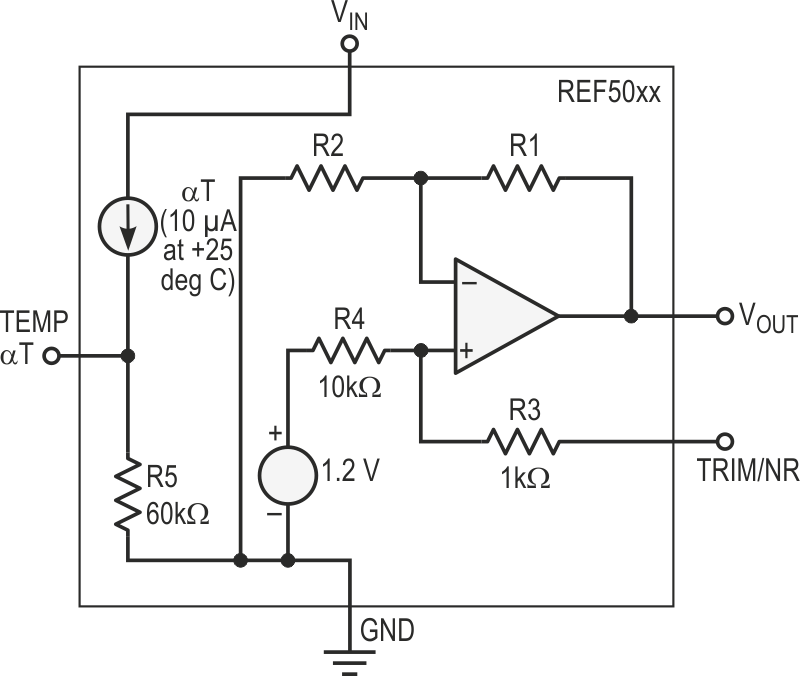
Texas Instruments’ REF50xx is a family of low-noise, low-drift, high precision series voltage references. Excellent temperature drift (3 ppm/°C) and high accuracy (0.05%) are achieved using proprietary design techniques.
Fig. 1 shows a simplified block diagram of the REF50xx family that provides a very accurate voltage output. However, VOUT can be adjusted to reduce noise and shift the output voltage from the nominal value by configuring the trim and noise reduction pin (TRIM/NR, pin 5). The TRIM/NR pin provides a ±15-mV adjustment of the device bandgap, which produces a ±15-mV change on the VOUT pin.
 |
||
| Figure 1. | REF50xx references are capable of both sinking and sourcing, and are very robust with regard to line and load changes. |
|
A supply bypass capacitor ranging between 1 µF to 10 µF is recommended. A 1 µF to 50 µF, low-ESR output capacitor (CL) must be connected from VOUT to GND. It must be less than or equal to 1.5 Ω. The ESR minimizes gain peaking of the internal 1.2-V reference and thus the REF50xx allows access to the bandgap that reduces noise at the VOUT pin. Placing a capacitor from the TRIM/NR pin to GND in combination with the internal 1-kΩ resistor creates a low-pass filter that lowers the overall noise measured on the VOUT pin. A capacitance of 1 µF is suggested for a low-pass filter with a corner frequency of 14.5 Hz. Higher capacitance results in a lower cutoff frequency.
There are seven different output voltage versions providing 2.048, 2.5, 3.0, 4.096, 4.5, 5.0, and 10 V. Each reference voltage is available in both standard and high-grade versions. They are offered in SO-8 packages and are specified from –40 °C to +125 °C.