Jess Espiritu, Analog Devices
Analog Dialogue
Introduction
Power-supply sequencing is required for microcontrollers, FPGAs, DSPs, ADCs, and other devices that operate from multiple voltage rails. These applications typically require that the core and analog blocks be powered up before the digital I/O rails, although some designs may require other sequences. In any case, proper power-up and power-down sequencing can prevent both immediate damage from latch-up and long-term damage from ESD. In addition, sequencing the supplies staggers the inrush current during power-up, an especially helpful technique in applications operating from current-limited supplies.
This article discusses the advantages and disadvantages of using discrete components to sequence the power supplies, and describes a simple, yet effective, method of achieving sequencing by using the internal precision enable pins of the ADP5134, which combines two 1.2-A buck regulators with two 300-mA LDOs. It also shows some sequencer ICs that may be useful for applications that require more accurate and flexible sequencing.
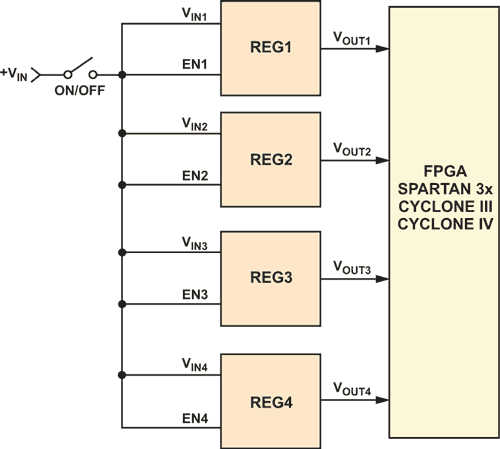
Figure 1 shows an application that requires multiple supply rails. These rails are the core supply (VCC_INT), I/O supply (VCCO), auxiliary supply (VCC_AUX), and system memory supply.
 |
|
| Figure 1. | Typical method for powering processors and FPGAs. |
As an example, the Xilinx® Spartan-3A FPGA has a built-in power-on reset circuit that ensures that all supplies have reached their thresholds before it allows the device to be configured. This reduces the strict requirement for power sequencing, but to minimize inrush current levels and observe sequencing requirements of circuits attached to the FPGA, the supply rails should be powered up as follows: VCC_INT → VCC_AUX → VCCO. Note that some applications require specific sequences, so always read the power requirements section of each data sheet.
Simple Power-Supply Sequencing Using Passive Delay Networks
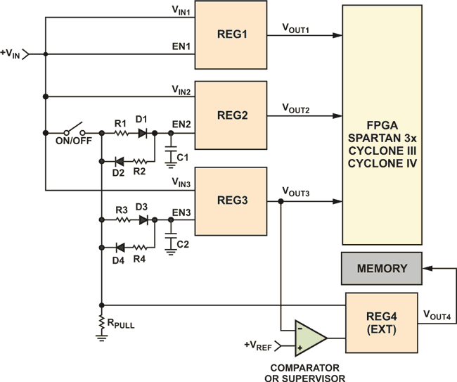
A simple way to sequence power supplies is to delay the signal going to a regulator’s enable pin with passive components such as resistors, capacitors, and diodes, as shown in Figure 2. When the switch closes, D1 conducts while D2 is left open. Capacitor C1 charges, with the voltage at EN2 rising at a rate determined by R1 and C1. When the switch opens, capacitor C1 discharges to ground through R2, D2, and RPULL. The voltage at EN2 falls at a rate determined by R2, RPULL, and C2. Changing the values of R1 and R2 changes the charging and discharging times, thereby setting the regulator’s turn-on and turn-off times.
 |
|
| Figure 2. | Simple power-supply sequencing method uses resistors, capacitors, and diodes. |
This method may be useful for applications that don’t require precise sequencing, and some applications, where simply delaying signals is sufficient, may require only the external R and C. The disadvantage of using this method with standard regulators is that the logic threshold of the enable pins may vary widely with voltage and temperature. In addition, the delay in the voltage ramp depends on the values and tolerances of the resistor and capacitor. A typical X5R capacitor will vary by about ±15% over the –55 °C to +85 °C temperature range and another ±10% due to DC bias effects, making the timing imprecise and sometimes unreliable.
Precision Enables Make Sequencing Easy
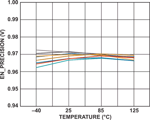
In order to get stable threshold levels for precise timing control, most regulators require an external voltage reference. The ADP5134 overcomes this problem by integrating a precision reference, saving significant cost and PCB area. Each regulator has an individual enable input. When the voltage at the enable input rises above VIH_EN (0.9 V minimum), the device comes out of shutdown and the housekeeping block is turned on, but the regulator is not activated. The voltage at the enable input is compared to a precise internal reference voltage (0.97 V typical). Once the voltage at the enable pin goes above the precision enable threshold, the regulator is activated and the output voltage starts to rise. The reference varies by only ±3% over input voltage and temperature corners. This small range ensures precise timing control, resolving the issues seen with using discrete components.
 |
|
| Figure 3. | Precision-enable turn-on threshold over temperature, 10 samples. |
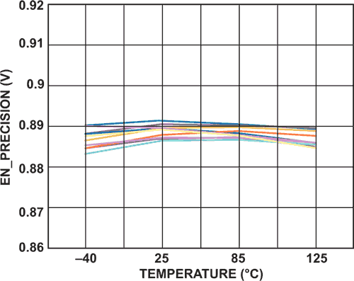
When the voltage at the enable input drops 80 mV (typical) below the reference voltage, the regulator is deactivated. When the voltage on all enable inputs drops below VIL_EN (0.35 V maximum), the device enters shutdown mode. In this mode, the current consumption falls to less than 1 μA. Figure 3 and Figure 4 demonstrate the accuracy of the ADP5134 precision-enable thresholds for Buck1 over temperature.
 |
|
| Figure 4. | Precision-enable turn-off threshold over temperature, 10 samples. |
Simple Power-Supply Sequencing Using Resistor Dividers
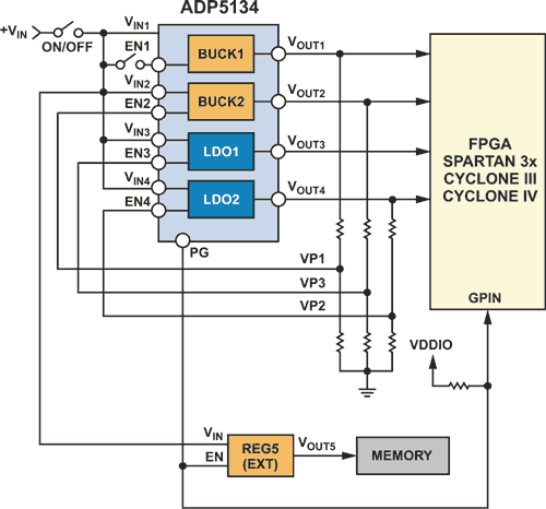 |
|
| Figure 5. | Simple sequencing with the ADP5134. |
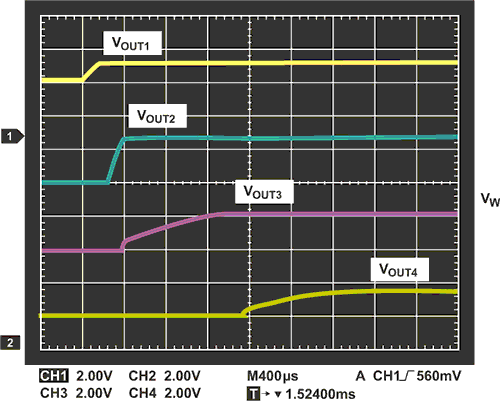
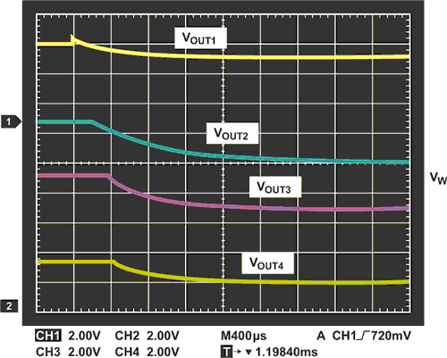
Multichannel supplies can be sequenced by connecting an attenuated version of one regulator’s output to the enable pin of the next regulator to be powered up, as shown in Figure 5, where the regulators turn on or off sequentially: Buck1 → Buck2 → LDO1 → LDO2. Figure 6 shows the power-up sequence after EN1 is connected to VIN1. Figure 7 shows the power-down sequence after EN1 is disconnected from VIN1.
 |
 |
||
| Figure 6. | ADP5134 start-up sequence. |
Figure 7. | ADP5134 shutdown sequence. |
Sequencer ICs Improve Timing Accuracy
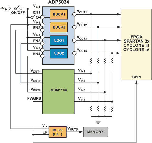
In some cases, achieving precise timing is more important than reduced PCB area and cost. For these applications, a voltage monitoring and sequencer IC such as the ADM1184 quad voltage monitor, which offers ±0.8% accuracy over voltage and temperature, can be used. Or, the ADM1186 quad voltage sequencer and monitor with programmable timing may be useful in applications that require more elaborate control of the power-up and power-down sequence.
 |
|
| Figure 8. | Sequencing the ADP5034 4-channel regulator using the ADM1184 quad voltage monitor. |
The ADP5034 4-channel regulator includes two 3-MHz, 1200-mA buck regulators and two 300 mA LDOs. A typical sequencing function can be implemented by using the ADM1184 to monitor the output voltage of one regulator and provide a logic-high signal to the enable pin of the next regulator once the output voltage being monitored reaches a certain level. This method, shown in Figure 8, can be used with regulators that don’t provide a precision-enable function.
Conclusion
Sequencing using the ADP5134’s precision-enable inputs is simple and easy to implement, requiring only two external resistors per channel. More elaborate sequencing can be achieved by using the ADM1184 or ADM1186 voltage monitors.
References