Volker Rzehak, Texas Instruments
Texas Instruments recently announced a new microcontroller family that implements FRAM as non-volatile memory instead of Flash, today's most common programmable, non-volatile memory technology. The paper explains the FRAM technology and how embedded applications can benefit from it.
The physics behind the FRAM technology are briefly covered. The differences and benefits of FRAM versus other non-volatile memory technologies like Flash are shown like the low current consumption, the fast write, and the high write endurance. The concept of "universal memory" is also introduced.
This paper illustrates how embedded applications can benefit from the features the FRAM technology offers such as ultra-low power data loggers and batteryless energy harvesting applications.
What is FRAM?
FRAM stands for Ferroelectric Random Access Memory. (Note there are other acronyms for FRAM used by other companies such as F-RAM or FeRAM.)
As the "RAM" part of the name already suggests, FRAM behaves similarly to DRAM. It allows random access to each individual bit for both read and write. Unlike EEPROM or Flash memory technology, FRAM does not require a special sequence to write data nor does it require a higher programming voltage. But FRAM is non-volatile; that is, it does not "lose" its content when power is removed.
So why is FRAM non-volatile? This is because of the special dielectric material used in the storage capacitor: a ceramic that allows making use of the so-called ferroelectric effect.
The term "ferroelectric" does not mean that the memory contains iron (the chemical element Fe) nor does it imply that the memory can be influenced by magnetic fields. In fact it is immune to magnetic fields.
 |
|
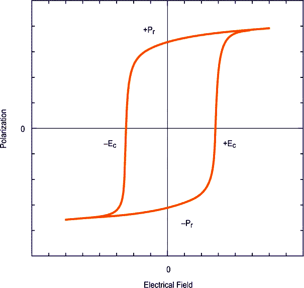
| Figure 1. | Polarization Hysteresis Loop. |
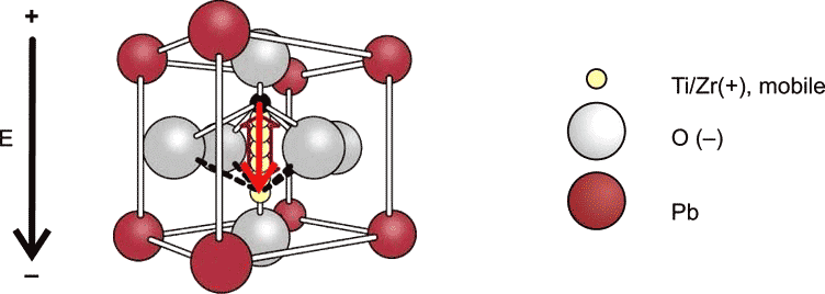
The term results from the hysteresis loop (shown in Figure 1) being similar to the magnetic hysteresis loop of iron (Fe). In contrast to the magnetic hysteresis loop, the one in FRAM results from the electrical dipole formed by zirconium (Zr) and oxygen (O) atoms in the ceramic lead-zirkonate-titanate crystal (PZT) used to implement FRAM as shown in Figure 2.
 |
|
| Figure 2. | Lead-Zirkonate-Titanate Structure. |
Applying an electrical field (E) can polarize the material by "moving" the Zi atom in the structure. But to move the Zi atom from one side (here from the upper) to the other side (here the lower) of the O atoms, it must cross the barrier from by the O atoms. So, with increasing field strength, the Zi atom moves gradually closer to the O atoms before – at a certain field strength – it "suddenly" flips to the other side. If a field is then applied with opposite direction, again the Zi atom would just gradually change its position before flipping to the other side. This will happen at the same field strength as before, but with an opposite sign. This behavior results in the electrical field versus polarization hysteresis loop shown in Figure 3.
 |
|
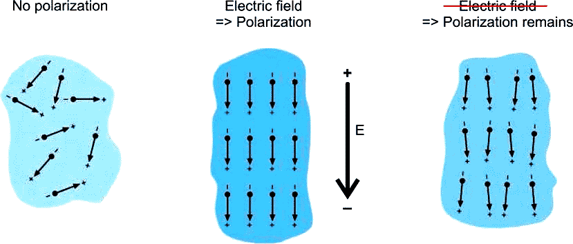
| Figure 3. | Polarization. |
After manufacturing, the dipoles formed by the zirconium and oxide atoms are randomly polarized resulting in a net polarization of zero (no polarization). Applying an electric field aligns the dipoles and results in a polarization in the direction defined by the electric field. Because the position of the zirconium atoms within the crystal structure is stable, the polarization remains even after removing the electric field.
Why FRAM? – An Application Example
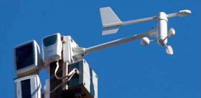
In the following example, the benefits of an FRAM-based microcontroller are illustrated using a data logger as application example. A data logger is typically a sensor node that collects various physical or environmental conditions like temperature, humidity, vibration, pressure, motion, or pollutants (see Figure 4).
 |
|
| Figure 4. | Data Logger. |
FRAM: A Universal Memory
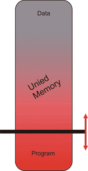
In a data logger application, the program code size required to measure and collect the data can be comparably small with respect to the amount of memory to store the data. Assuming the use of external memory is not an option and, thus, the data should be stored in the RAM of a "traditional" flash-based microcontroller, one would have to purchase a device that has excessive program memory compared to what the application needs. With an FRAM-based microcontroller, the available memory can be partitioned to the needs of the application and, thus, a much larger portion can be made available for data to meet the application requirements.
The concept behind this is called "unified memory" (Figure 4). Universal memory allows flexible partitioning of the memory for code and data: the same type of memory can be used for both data and program storage that are "traditionally" kept in separate memories: RAM for data and flash or ROM for program storage.
 |
|
| Figure 5. | Unified Memory. |
To support the "unified memory" concept, a Memory Protection Unit (MPU) is implemented in the FRAM-based MSP430 devices from Texas Instruments. The MPU allows for example to "protect" parts of the memory that are used for program storage from being overwritten accidentally.
Write Endurance
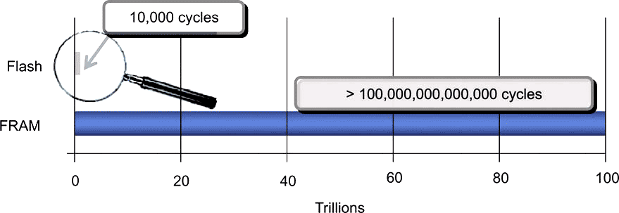
The FRAM technology provides write endurance that is superior to other non-volatile memory technologies as illustrated in Figure 6. For the data logger application, that translates into a much longer lifetime with less complexity: assuming the data logger has to store one set of data each second and it always uses the same addresses, this would translate into a lifetime of a data logger using Flash memory of less than three hours (assuming a Flash with 104 cycles divided by 1 cycle per second). The same data logger using FRAM would achieve a theoretical life time of more than 3 million years making use of the more than 1014 write cycles FRAM offers. To increase the life time of the Flash-based data logger, complex wear leveling algorithms together with additional Flash memory space would be required. The wear leveling algorithms would try to make use of multiple Flash cells and use them more or less equally. For FRAM, wear leveling is not required, which significantly reduces the complexity and also the amount of memory required.
 |
|
| Figure 6. | Write Endurance. |
Fast Write
An additional benefit of the FRAM technology is its fast write capability.
To write Flash, tens of microseconds to several milliseconds are required to program one data word (for example, the MSP430F5438A specifies between 37 µs and 85 µs to program one word, depending on programming mode and process conditions; for other microcontrollers, programming times in the range of 3 to 5 milliseconds are sometimes specified). This does not include a pre-erasure of the segment to be re-programmed. The pre-erasure will add several milliseconds. In addition, no program execution is usually possible while programming.
In contrast, FRAM requires only ~100 ns to program one data word. Additionally, no pre-erase is required and, because of the fast write, there is virtually no interruption of the program execution.
Another Application Example: Light Switch
The following application is a light switch that switches the lights via an RF link and harvests the energy from being switched. This means that the microcontroller and transceiver are not powered most of the time. Because of that, all data that needs to be retained must be stored in a non-volatile memory. The data that must be retained could be, for example, RF network parameters. In an intelligent light switch with dimming, additional status information could be stored.
In a flash-based microcontroller, the programming of a word would require a couple hundred nanocoulomb (nC) of charge (for example: ~100 µs × 2 mA = 200 nC), whereas in a FRAM-based microcontroller, the required charge to program the same amount of bits is on the order of two to three magnitudes (more than 100 times) smaller (for example: ~100 ns × 4 mA = 400 pC). Thus, with the same charge harvested from being switched, more than 100 times of data can be permanently stored with a FRAM-based microcontroller compared to a Flash-based microcontroller. Alternatively, the energy harvesting circuitry can be dimensioned to provide and store less energy.
Of course, this example is applicable to all energy harvesting applications that can be unpowered for a certain time but still need to retain variable data.
Note: the charge required to program can vary from device to device and from manufacturer to manufacturer. The numbers shown here are only examples used to show the magnitude of difference.
Other Applications
FRAM-based microcontrollers can be used for any application where microcontrollers with a different non-volatile memory technology like Flash or EEPROM are currently used. However, certain application can specifically benefit from the FRAM technology, and other applications might only be possible with FRAM as memory.
A few additional applications or application scenarios are listed that specifically can benefit from the features an FRAM-based microcontroller offers:
- Data logger applications
- Energy harvesting application
- Applications with "Over the Air Updates"
- Replacement of external EEPROM
MSP430FR57xx Family
Beyond integrating FRAM as their main memory technology, the MSP430FR57xx family devices have other unique features suck as an extremely low active mode current consumption of ~100 µA/MHz. They also offers a rich mixture of peripherals including communication ports, timers, and a 10-bit ADC with integrated reference.
The MSP430FR57xx family offers 20 different devices with FRAM memories up to 16kB. The devices are offered in four packages ranging from a tiny 24-pin QFN to a 40-pin QFN, as well 28-pin and 38-pin TSSOP packages.
Conclusion
A microcontroller with integrated FRAM provides a non-volatile memory that can be used for both data and code storage (unified memory), is low-power, can be written quickly, and offers practically unlimited write endurance.
The FRAM-based microcontrollers can be used in nearly every MCU-based application, and their unique features may enable new applications we currently might not even think of.
References
- TI's FRAM page: http://www.ti.com/fram
- General FRAM information at http://en.wikipedia.org/wiki/Ferroelectric_RAM
- MSP430FR57xx data sheet (SLAS639)
- MSP430F5438A data sheet (SLAS655)
