Tom Starnes
Digi-Key
Flash memory completely dominates microcontrollers (MCUs) now, but memory considerations have become more complex as the processors have advanced to 32-bit architectures and peripherals have become much more capable. It is easy to forget about memory among the exotic peripherals that make the MCU more of a system-on-a-chip (SoC) encompassing advanced motor control, graphical user interfaces (GUIs), and networking.
Still, the details of Flash and other memory types deserve attention to ensure that the selected MCU has memory that matches the needs of the system. Rapidly increasing use of the ARM Cortex-M processor architecture at higher speeds in MCUs also invites closer inspection of memory support. Vendors take different approaches to their on-chip memory options, which may tip the balance of which MCU to choose.
As much as a megabyte of Flash memory is available on larger MCUs today. The ratio of program store, data tables, and scratchpad RAM changed as MCUs found new applications and took on new functionality. Higher-end MCUs are probably programmed in a high-level language (HLL), running a real-time operating system (RTOS), and utilizing off-the-shelf stacks and software packages. Each of these factors affects memory needs and usage.
The Flash memory typically used on MCUs has access times that let it keep up with 25 to 50 MHz processor clocks. When high performance processor cores are clocked over 200 MHz, there could be a huge gap to fill with time- and power-consuming wait-states. Multiple on-chip buses and special routing mechanisms can be quite beneficial in alleviating the traffic problems in some busy microcontrollers.
The ARM processor core architecture has very good code density due to its compact Thumb2 instructions which require only 16 bits to store instructions rather than the expected 32 bits. The ARM Cortex-M0, Cortex-M3, and Cortex-M4 cores are popular in microcontrollers from numerous vendors, and some memory choices will be investigated here.
NXP Semiconductors LPC4000 – Real-time aids data processing
NXP Semiconductors has been successful with ARM-based microcontrollers since adapting ARM7TDMI cores for MCU use long ago. NXP quickly added the Cortex-M cores to its portfolio once they became available, and has been one of the leaders integrating the Cortex-M3, Cortex-M0, and Cortex -M4 into MCUs with high speed at one end while pushing prices lower at the other. NXP was one of the first to go to an extra-wide Flash memory organization to buffer subsequent memory locations to ensure availability without delay.
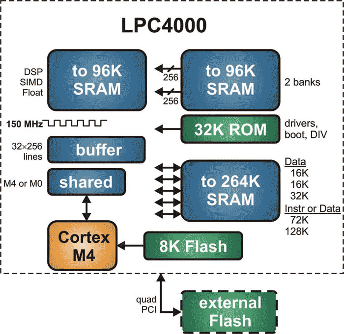
NXP's latest MCU family, the LPC4000 (see Figure 1), is interesting for a couple of reasons, such as the inclusion of a Cortex-M4 – which has digital signal processing (DSP), single instruction multiple data (SIMD), and optional floating-point instructions – as well as a separate Cortex-M0 processor core on each. To keep the Cortex-M4 fed fast enough, and to keep power consumption low, NXP expanded the on-chip Flash to 256 bits wide, the widest in the industry.
 |
|
| Figure 1. | NXP LPC4000 architecture (Courtesy NXP). |
NXP uses a fairly-straightforward buffer system to hold 32 lines of recent Flash memory accesses, giving immediate availability to recently fetched instructions. This provides more consistent execution performance than might be experienced using more exotic schemes. Some cache replacement algorithms can work against compiler-generated code and can be more difficult to simulate and debug. NXP finds execution from their Flash can run within five percent of the performance from RAM, running up to 150 MHz in the current 90 nm process.
Two banks of Flash give isolation and partitioning that also provide absolute confidence when re-Flashing one bank while the application continues to run from the other.
LPC4000s have up to 1 MB of Flash with a whopping 264 KB of SRAM on-chip – a 4:1 ratio of program to data memory. If desired, instructions can be executed directly from much of the RAM with zero wait-states – ideal for the fastest deterministic real-time processing without concern for code bouncing around at a fine-grain level. Assortments of SRAM blocks are available, so different routines and input/output (I/O) do not fight for bus time.
It is easy to use inexpensive external Flash memory with the LPC4000 for expansion program space, code that will be copied into SRAM first for fastest execution, or even large graphics images destined for display screens. Readily available Flash with a serial peripheral interface (SPI) port, including quad-SPI Flash, can actually be direct-mapped into the normal memory space of the processor, and the programmer does not have to think whether it is on-chip or connected serially off-chip. The SPI Flash interface (SPIFI) offers four lanes to external Flash, and allows images in Flash to be DMA'd directly to the LCD controller at up to 40 MBps.
The Cortex-M0 has its own 8 KB program memory and passes messages to the bigger brother Cortex-M4, via shared memory.
This series of MCUs also includes 32 KB ROM containing software drivers, boot code, and other handy bits of code to relieve the system designer from having to write this code and leaving more precious Flash for more application-specific routines. The speed and power efficiency of ROM execution is naturally better than Flash as well. A library to perform dependable fixed-time DIVIDE operations is offered with some MCUs.
NXP's earlier versions of ARM Cortex MCUs may be on larger 180 nm or 140 nm process nodes, and most utilize a 128-bit wide Flash rather than the 256-bit architecture just described. All the Flash was developed by NXP specifically for MCUs, and it has built-in single-error correction/double-error detection with logging for better Flash integrity and monitoring. NXP has a broad spectrum of ARM-based MCUs that incorporate the Cortex-M0, Cortex-M3, and Cortex-M4, with the smallest fitting into just 16-pin packages and selling at prices one would expect for 8-bit MCUs.
