Jack G. Ganssle
Embedded Systems Design
64-bit CPUs and VLIW architectures slam massive amounts of data around via wide parallel buses. Processors today are so fast and so hungry for data that chip designers do horrible things to push bits into the CPU as quickly as possible. But at one time, a narrow bus was seen as a competitive advantage.
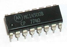
Motorola’s MC14500 was a onebit CPU the company called an “Industrial Control Unit.” The device’s handbook has the intriguing statement: “When a job is dominated by calculations or data logging, a multibit processor is appropriate. When the task is decision and command oriented, a one-bit machine is an excellent choice.”

I can’t determine when the chip came to market, but the handbook is dated 1977. Revision 3 of the datasheet was released in early 1994, so these odd devices did gain some traction. Rumor has it they were used in some HVAC systems and in a lot of ladder-logic applications. Indeed, the part’s handbook goes on at great length about implementing ladders in MC14500 assembly language.
This was a very early Harvard architecture part in that there were two buses: one 4 bits wide for instructions and a single-bit data bus. So, although the “one-bit” moniker is somewhat correct, the device was a bit schizophrenic.
The MC14500’s 16 instructions did not include any arithmetic operations. No add, subtract, or the like. Instead, it included some simple loads and stores, ANDs and ORs, a jump, a single conditional skip, and a few åinstructions to control hardware. (It’s possible to do arithmetic using just logical instructions.)
Only a single register – the Results Register – existed, and that was, of course, just a bit wide.
This part was so quirky it didn’t have a program counter. Designers were expected to create one external to the CPU. Its width was, well, anything the developer wanted. Running a tiny bit of code? Maybe an 8-bit PC was appropriate. Or 32 bits for those applications needing 4 GN (giga-nibbles) of powerhouse processing.
 |
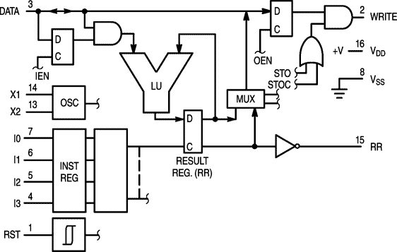
| The MC14500B block diagram |
So the inevitable question is “how did a jump work?” That was entirely up to the engineer crafting the circuits. The output enabling instruction (OEN) could be used to disable any changes occurring on the output data; at the end of a loop, assert OEN and let the machine execute whatever instructions – hopefully NOPs – remained until the PC rolled over. There was a JMP, but that instruction simply toggled an output bit. The design engineer was supposed to make that signal do something useful, like load the PC with some address.
As they would say here in Finksburg: “them boys at Motorola musta been smokin’ somethin’ illegal.”
