Engineers just love to put shields on circuits, mostly as a defensive measure against signals on the outside getting into and disturbing our circuits, but they also keep signals inside from getting out and this really makes the folks responsible for EMI compliance happy.
Even on low-frequency circuits, shielding can take care of drift due to air currents and AC power mains pickup. At higher frequencies shielding can take care of emissions and pickup. In RF or microwave circuits shielding makes possible radio receivers, spectrum analyzers and all sorts of equipment that simply would not function without sufficient shielding and the isolation that it provides between the various RF and IF sections.
So what could go wrong? Well 10 years ago, not much. We were still working at frequencies up to 2.5 GHz for almost all the standard wireless applications. And shields generally only helped the situation. Then we considered “commonplace RF” to be anything below 3 GHz, but today we consider “commonplace” to be below 6 GHz, and we may routinely need to lay out circuits that operate to 6 GHz even in consumer circuits [1].
This situation demands shielding our RF circuits, not only to keep our circuits working properly, but to prevent EMI emissions failures during regulatory testing.
The usual form of shielding is some sort of conductive structure placed over our circuit. These can range from TV tuner types of cans, simple plastic moldings that have been coated with conductive material, or expensive machined chunks of aluminum, purpose made just for our circuit board.
When we place a shield on a circuit board we are creating a conductive electrical cavity and this cavity likes certain frequencies or various TEM (Transverse ElectroMagnetic) modes [2]. In other words it becomes resonant at certain frequencies.
These resonance modes are usually bad, because we wanted our shield to stop electrical fields from escaping (and that it does), but at certain frequencies, inside the shield, the electromagnetic waves get quite vigorous at certain frequencies. This is where our problems can start.
It is possible to predict the frequencies where this starts to happen by using simple math [2].
For a box of dimensions H, W and L (for Height, Width and Length), and where W > L > H), the various TEM modes can be calculated by the equation:
 |
(1) |
where
the dimensions are in meters,
the calculated Resonance Frequency is in MHz
and the medium inside the shield or cavity is assumed to be air.
Variables a, b and c take on the various TEM modes – they are either 1 or 0. With three possible variables either 1 or zero, this simple model can be used to predict all possible TEM modes for a rectangular closed box.
In shielding design we are typically only interested in the lowest frequency that the shield cavity can resonate at, so Equation 1 can be simplified to,
 |
(2) |
Equation 2 represents TEM101 Mode. The 'a' and 'c' of equation 1 are made equal to 1 and 'b' is 0. As you can intuitively see, this is the diagonal of the shield's largest dimensions. And the inverse of this diagonal length would be proportional to frequency.
Equation 2 then can be used to calculate the lowest frequency at which a rectangular shield will resonate.
Testing Theory and Practice
We now have a way to see if our shield will resonate at some low-enough frequency that we care about; let's do some real testing. I routinely use these little box shields that can be soldered to a PCB [3]. A small shield that I regularly use measures 1.5×1×0.4 inches. Using these dimensions with Equation 2 we find that the lowest-frequency TEM mode is at about 7 GHz.
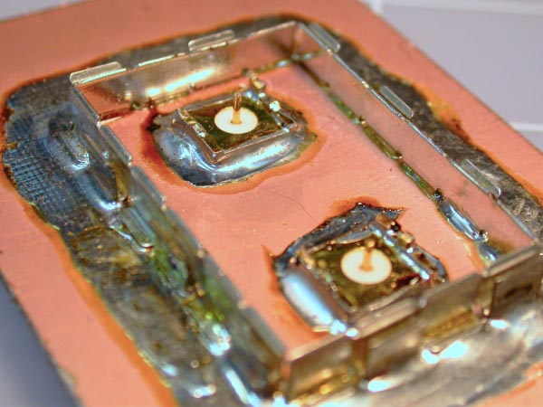
To test this out, I built a test circuit that consists of an input probe, an output probe and a shield soldered to a piece of scrap circuit board (Figure 1).
 |
|
| Figure 1. | To test this theory out, I soldered a 1.5 x 1 x 0.4-inch metal shield on a piece of circuit board material. To get signals in and out I also soldered some modified SMA PCB connectors to the inside of the shield cavity. These act as small capacitive probes and allow us to take a quantitative look inside the shield when connected to a Vector Network Analyzer (VNA). |
No particular attention was given to the length of the center conductor probe, other than to make them short electrically (<< ¼ wavelength at the frequencies of interest). They were mounted just at the ends of the box somewhat randomly. The ends of the box were chosen for the probe locations as this perhaps represents the best hoped for isolation inside of a shield, the ends possibly representing the input and output points of a particular circuit, etc.
 |
|
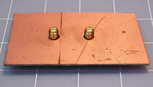
| Figure 2. | This is the backside of the test board showing the SMA connectors that will attach to my Vector Network Analyzer for analysis. |
 |
|
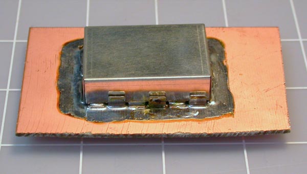
| Figure 3. | This is what the test setup looks like with the shield cover in place. |
Time to make some real measurements. A VNA was connected between the connectors and the VNA's port 1 and port 2. Then a series of S21 measurements were made.
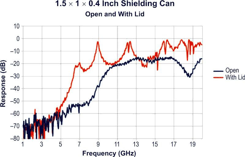
The first plot on the VNA was with the lid off, and it shows the natural coupling between the input and output probe (Figure 4). This circuit could be roughly modeled with a small capacitor in series with a resistor between the circuit probes inside the shield. At low frequencies the coupling is very small, while at higher frequencies the coupling increases and eventually levels off.
Needless to say, the exact location of the capacitive probes in the shield will effect the exact response. Closer together and the coupling will increase, etc. But as long as we don't move the probes the comparison results will be valid, and these probes are soldered in place, so they don't move.
 |
|
| Figure 4. | The Blue trace is a VNA plot of the input to output with the cover off. This shows the expected capacitive coupling behavior until very high frequencies. The Orange trace is what happens when the lid is put on, this completes the cavity circuit and turns our tame circuit board into a the highly resonant and complex cavity structure with multiple resonances. |
As can be seen in Figure 4, when the lid is put on, our nice shielding box turns into a complex resonant structure with multiple resonances (peaks and dips). Equation 2 predicted that the first resonance would happen at about 7 GHz and sure enough, that is where the first peak is. At that first peak the coupling between the input to output probe has been reduced by over 30 dB.
Why care about this? There are a number of reasons. First, if you have gain at any of these peaks the increased coupling can cause a spurious oscillation. This may be out of your band of interest, but if your amplifier is oscillating at some high frequency it will probably be detrimental to its operation at lower frequencies also.
I once had a multistage amplifier that oscillated well out of band when it was buttoned up in its shield. You would never see it in a VNA gain or match sweep, but it changed the amplifier's operating point and also the harmonics of the amplifier and that did affect the downstream circuits.
If, on the other hand, your circuit operates through these resonances it is possible that as you sweep the frequencies through these points you will see all sorts of unexplained power dips (also called “suck outs”).
A third problem may be when your circuit has internal frequencies near these resonances (or just by the increased broadband coupling). This peaks the energy inside the shield and can cause EMI emissions failures by increasing the leakages that get outside the shields.
I am sure that there are countless others; these are just a few of the ones that have caused me grief.
References:
- 802.11 Wireless routers can be bought at Home Depot that operate in the 5.8-GHz band. Such electronics are pretty commonplace when you can buy it at the Home Depot.
- See any college textbook on fields and waves for an in-depth explanation of this topic. Such as: Lines, waves and antennas, Robert Brown, et al. 1973
- Leader Tech is the supplier of the shield that was used in this example, leadertechinc.com
