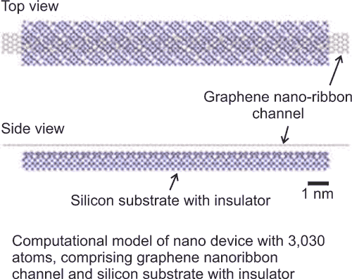
Supercomputer used to calculate electrical properties in approximately 20 hours
Fujitsu Laboratories Ltd. announces that it has successfully simulated the electrical properties of a 3,000-atom nano device – a threefold increase over previous efforts – using a supercomputer. At the nanoscale level, even minor differences in the local atomic configuration can have a major impact on the electrical properties of a device, requiring the first-principles method [1] of calculation to be used to accurately compute physical properties at the atomic level. However, when applying this method to electrical property forecasting, the massive computations involved limit these forecasts to the order of 1,000 atoms.
Fujitsu Laboratories has now developed a calculation technique that reduces memory requirements while maintaining precision. Application at a 3000 atom scale have been made possible through a supercomputer using massively parallel processing. This technique enables the calculation of electrical properties, not only of individual nano device components, but of the interactions between these components. Expectations are that this development will contribute to faster practical implementations of nano devices. This simulation used massively parallel computing technology developed by the Japan Advanced Institute of Science and Technology (JAIST) and the Computational Material Science Initiative (CMSI).
Details of this technology are being published in the January 14 edition of the Applied Physics Express (APEX), the letter journal of the Japan Society of Applied Physics.
Background
As silicon devices such as LSI have become increasingly compact, there has been a heightened level of both operating speed and energy-efficiency. In recent years, however, with the limits of miniaturization continuing to draw near, it has become an increasing challenge to squeeze additional performance from chips. This has led to fervent efforts to develop devices made from new materials and new types of structures.
Technological Issues
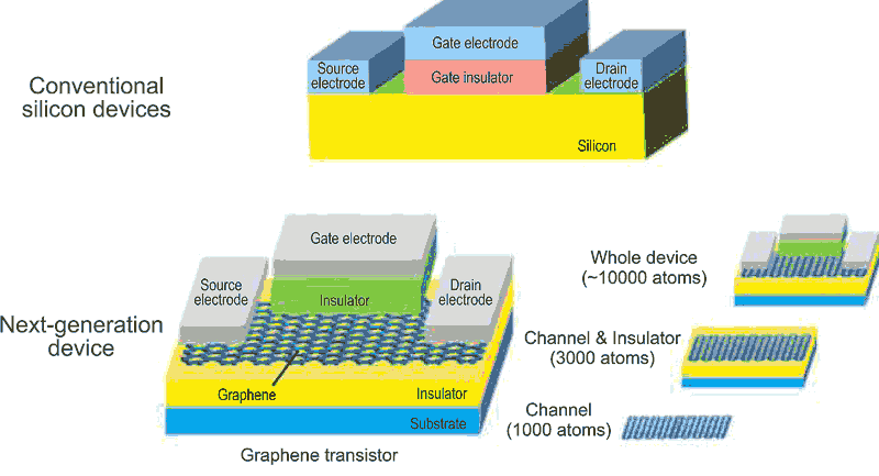
Simulating a nano device's electrical properties accurately on a computer rather than through experimentation can make the development process quicker and less expensive. An effective way to do this is to derive the electrical properties from the first-principles method, which accurately calculates the behavior of each atom. But as the first-principles method requires a massive amount of calculations, applying it to electrical property forecasting is limited to models on the scale of 1,000 atoms (Figure 1). On this scale, only channel regions – the pathways for electricity – can be calculated. A simulation that would include interactions with thousands of adjacent electrodes and insulators – which are thought to greatly affect electrical properties – has been impossible.
 |
|
| Figure 1. | Conventional silicon devices and next-generation devices. |
About the Technology
Fujitsu Laboratories has developed a computational technique that reduces memory requirements while preserving accuracy. Along with the use of a massively parallel supercomputer, this has made it possible to derive the electrical properties of a 3,000-atom nano device using the first-principles method. Simulating the electrical properties of a 3,000-atom nano device was accomplished in approximately 20 hours.
 |
|
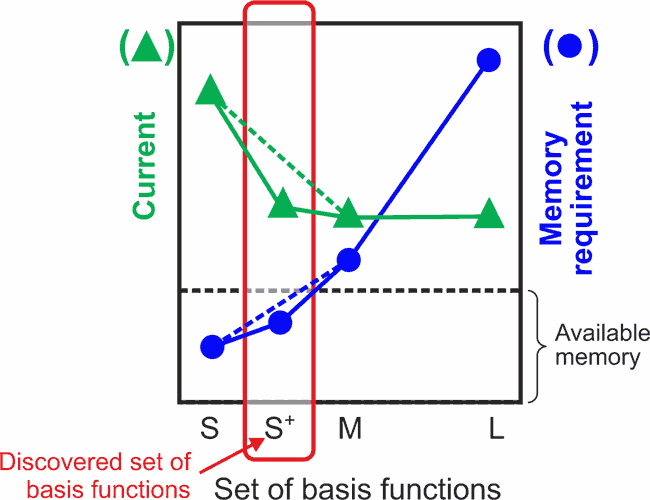
| Figure 2. | Results from the newly discovered set of basis functions. |
The simulation uses a set of basis functions that represent the flow of electricity. Typically, increasing the number of basis functions enhances the accuracy in approximations of the actual electrical current, but it also boosts the amount of memory used for the computation. A detailed study of these results, from a physical-sciences perspective, led to the discovery of a set of basis functions that holds the required memory to less than the available memory (Figure 2).
 |
|
| Figure 3. | Sample atom partitioning of carbon nanotubes. |
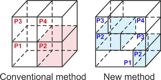
In performing the simulations, Fujitsu Laboratories used OpenMX [2] , software for calculations with first principles that uses massively parallel technology developed by JAIST and the CMS Initiative. This program used an atom-partitioning technique (Figure 3) to limit the memory and communications demands, and a space-partitioning technique (Figure 4) to accelerate fast Fourier transform calculations, which are a key part of calculations from first principles.
 |
|
| Figure 4. | Spatial partitioning method for 3D fast Fourier transform. |
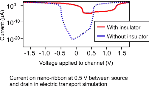
This combination of techniques made it possible to simulate the electrical properties of a nano device with 3,030 atoms, comprising both graphene and an insulating layer, in approximately 20 hours on a supercomputer [3]. Simulation results with and without the insulating layer are shown in Figure 5.
|
|||
| Figure 4. | Simulation results. | ||
Results
This technology, being capable of modeling the electrical properties of a 3,000-atom nano device, was used to discover the electrical properties of a nano device that included interactions with its environment, making a significant step toward the design of new nano devices.
Future Plans
Based on development of ever-more massive parallel computing technology that has kept pace with the performance increase of computers, Fujitsu is pursuing larger-scale and more efficient calculations. Within the next several years, Fujitsu aims to achieve nano device design via computers through total simulations of nano devices (on the scale of 10,000 atoms).
Glossary and Notes
- First principles: Rather than using experimental data and empirical parameters, this is a method that calculates physical properties from the basic laws of quantum mechanics that govern atoms and electrons.
- OpenMX: Open-source package for Material Explorer.
- Approximately 20 hours on a supercomputer: Using a 3,000-core Fujitsu PRIMEHPC FX10 supercomputer.
