Michael Kugelman
Power Electronics
Two new patented circuits control AC power to resistive and reactive loads with minimal EMI. They are applicable to single and multiple AC phases and varying AC frequencies.
Switching AC power on and off has been a challenge since Edison and others started switching power more than 125 years ago. Now, a solid-state relay (SSR) uses a patented zero-voltage crossing technique to switch AC power on and off while producing minimal EMI.
To see how this SSR technique works, we must examine the ways to switch AC power. Semiconductor technology increasingly has displaced electromechanical relays. Semiconductors used in SSRs typically fall into two types: thyristors (SCRs, Triacs, etc.), and transistors (bipolar types, MOSFETs, IGBTs, etc). Thyristors are triggered on and stay on until a zero-current crossing turns them off while transistors are commanded on and off at any time by control signals.
SCRs used in the SSRs can switch AC power, but it takes two SCRs wired in inverse parallel to control both directions of the AC. It's harder to turn off an SCR in the middle of a cycle, because it latches itself on and must be forcibly commutated off. It's also harder to connect SCRs in parallel to share the current and reduce heat dissipation due to their tendency to current hog with increasing temperature. SCRs also are sensitive to the dv/dt of the line, and care must be taken to ensure they don't turn on inadvertently.
Triacs used in SSRs reduce part counts because they basically are two SCRs wired in inverse parallel. However, Triacs have a very small time window at the zero crossing to commutate off and thus aren't often used in higher frequency applications due to the possibility of staying turned on. To prevent this, snubbing circuits often are employed to reduce the dv/dt seen by the device. Triacs also are harder to connect in parallel for the same reasons as SCRs.
MOSFETs increasingly are being used in AC applications because they are easy to connect in parallel, which can result in a lower voltage drop and less heat dissipation than SCRs or Triacs. In addition, the MOSFETs can be turned on and off at any time. Also, they do not share the dv/dt problems of SCRs and Triacs.
EMI
Switching a relay on and off in AC circuits generates undesirable EMI. An electromechanical relay can generate a large amount of noise due to the bouncing of the contacts and is why an SSR is often selected when low EMI is needed. Phase control switching of the SSR can also cause EMI.
Each time a thyristor is triggered in a purely resistive circuit, the load current goes from zero to the load limited current value in less than a few microseconds. This produces an infinite spectrum of energy, with an amplitude inversely proportional to frequency. With full wave phase control in a 60-Hz circuit, there is a pulse of this noise 120 times a second. In applications where phase control is used in the home, this can be annoying, because the frequencies can interfere with the broadcast band of AM radio.
Reducing or eliminating EMI is desirable. One common technique is zero-voltage switching (ZVS), which ideally consists of closing the contact to the load at the instant the voltage across it is zero and opening it when the current through the load is zero (for resistive loads these points are the same). This approach yields the lowest possible di/dt and ensures a minimal generation of high-frequency switching components. Most SSR circuits currently produced do not detect a true zero-voltage crossing, but instead are operated when the voltage is between 5 V and 12 V. If low EMI is required, especially with high load current, then this 5-V to 12-V window threshold for the zero crossing may not be satisfactory.MOSFETs can also be used back-to-back to control the AC. Power MOSFETs generally control current in only one direction. However, by placing them back-to-back, they can be used to control both directions of AC power.
Turning the MOSFETs on quickly at the zero-voltage crossing to minimize EMI presents some difficulty because of the inherent inaccuracies of timing the MOSFET to achieve switching exactly at the zero crossing of the power line. When a MOSFET is turned on, it usually is not at the zero-voltage crossing due to the inherent delay between the command and the MOSFET turn-on time.
TATTOO Technique
A way to solve this is a novel alternate transistor turn-on and -off technique that places a diode in parallel with each back-to-back MOSFET, which takes advantage of the normal commutation of diodes to generate a near-perfect zero crossing. This zero-voltage crossing technique of alternate transistor turn-on and -off is called TATTOO (Technique of Alternate Transistor Turn On and Off). It is relatively insensitive to the power supply frequency and can be designed for a number of phases or supply voltages.
When the circuit is given the command to begin operation, the basic scheme is to turn one MOSFET on while the other MOSFET is off (in its blocking mode). This allows current to flow in only one direction, but this will not happen until the zero-voltage start of the first voltage cycle. The other MOSFET then will turn on during the first cycle when the ac voltage switches polarity to eventually allow current to flow in the reverse direction. The parallel-connected diodes allow current to flow until the second MOSFET is turned fully on and carries the load current. This eliminates the critical timing needed to turn on the MOSFET at the zero crossing of the voltage supply, because the diode naturally commutates on and carries the current until the MOSFET is fully turned on. The opposite circuit operation to achieve the same zero-voltage crossing result occurs when the load current turns off.
 |
 |
||
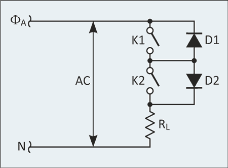
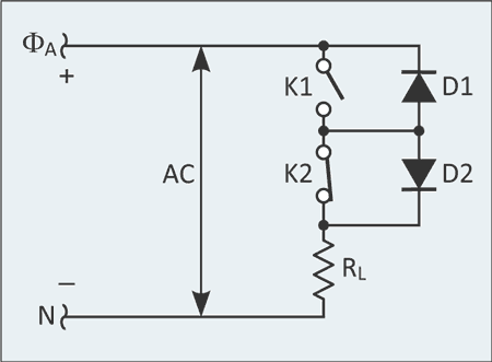
| Figure 1. | The state of switches K1 and K2 when the SSR is off. | Figure 2. | When K2 is closed, the SSR is on. Phase A is positive, so D1 blocks and no current flows. |
Fig. 1 shows the state of the circuit when the FETs (K1 and K2) are off. The diodes block in both directions so no current flows to the load (RL). When K2 is closed (Fig. 2), the SSR is on. Phase A is positive so D1 blocks and no current flows. K2 can be turned on slowly (several hundred microseconds); because the blocking diode (D1) will not allow the current to flow so the speed or accuracy of turning on K2 is not crucial.
 |
 |
||
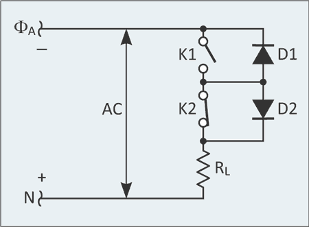
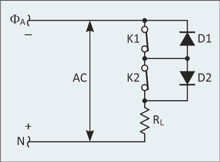
| Figure 3. | When phase A goes negative, current flows immediately, starting at the zero crossing, through K2 and D1. | Figure 4. | When K1 finally closes, current flows primarily through K1 and K2 in both directions in phase with the supply voltage. |
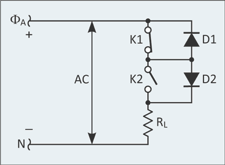
When phase A goes negative (Fig. 3), current flows immediately, starting at the zero crossing, through K2 and D1. During this first cycle of operation, K1 can be turned on slowly. Fig. 4 shows the state of the circuit when K1 finally closes. Current now flows primarily through K1 and K2 in both directions in phase with the supply voltage. Fig. 5 shows the sequence when the SSRs are turned off. When phase A becomes positive, K2 can be opened slowly and D2 will carry the current. (This doesn't interrupt the current until the next step.)
 |
 |
||
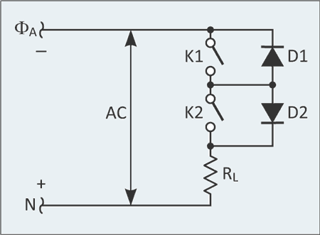
| Figure 5. | When the SSR is off and phase A becomes positive. K2 can be opened slowly and D2 will carry the current. | Figure 6. | When phase A goes negative. K2 is open and D2 is now blocking, so (he load current ceases and K1 can be turned off slowly. |
When phase A goes negative in Fig. 6, K2 is open and D2 is now blocking, so the load current ceases and K1 can be turned off slowly (several hundred microseconds, for example).
The end result is a load current that starts and stops with no discernible “step” at the zero crossing points. An additional feature is inherent “integral cycle control” (i.e., only full cycles are delivered to the load), a desirable feature when used with loads that are sensitive to magnetic flux saturation.
Resistive vs. Reactive Circuits
Current and voltage are in phase in a resistive circuit. Thus, there is no problem turning the switch on and off at these zero-voltage points because that's when the voltage and current are zero. However, in a reactive circuit, the voltage and current are not in phase, and the switch must be operated on at the zero-voltage point and off at the zero-current point.
 |
|
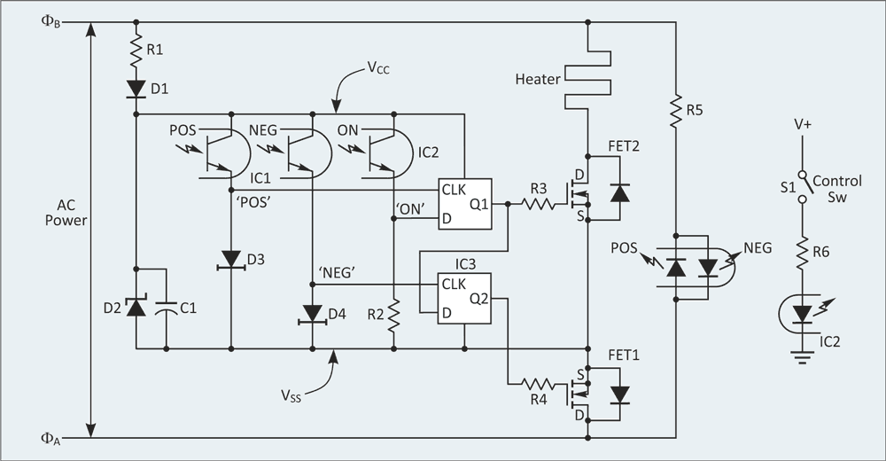
| Figure 7. | The actual TATTOO circuit. |
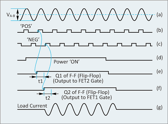
Fig. 7 shows an actual circuit, and its timing diagram is shown in Fig. 8. The floating VCC in Fig. 7 is referenced to the sources of the two MOSFETs so that any command signals will be properly referenced. Diode (D1) half-wave rectifies the AC through (R1 and D2) and the parallel connected diode (in FET1). C1 holds up the VCC during the AC reversal. The values of these components will vary depending on the AC voltage and frequency and the acceptable ripple on VCC.
 |
|
| Figure 8. | Timing diagram for the TATTOO circuit. |
Optocoupler IC1 develops pulses (“POS” and “NEG”) when phase A goes positive or negative with respect to phase B. These pulses appear at the anode of D3 and D4 (active pull-down devices) and are fed to the clock inputs of the two flip-flops of IC3. One pulse appears every half cycle of the AC waveform, so the flip-flops are clocked at alternate half cycles. As long as IC2 is not on, R2 pulls the data line of the top flip-flop low, and each clock pulse will clock a low to the Q1 output keeping FET2 off. Q1 is also fed to the data input of the lower flip-flop and because it is low, FET1 will be off.
 |
|
| Figure 9. | Scope traces show the time relationship of the ON command to the power line voltage and the turn on and off of the load current |
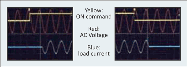
This state of affairs continues until S1 (control switch) is turned on. When S1 is turned on, optocoupler IC2 turns on, and a high signal (“ON”) is applied to the D input of the top flip-flop. The next time a “POS” pulse appears, it clocks “ON” into the flip-flop setting Q1 high and turns on FET2. Phase A is positive at this time, so no current will flow through the load (blocked by FET1). Q1, however, is now high and is applied to the data line of the lower flip-flop. At the next phase reversal of the power line (“NEG”), “ON” will be clocked into the lower flip-flop and sets Q2 high, turning on FET1. Although the FET won't turn on immediately, the parallel diode will, and FET1 will conduct fully sometime later in the half-cycle, but the time is not critical. The circuit is now fully conducting and will turn off in the reverse order when the control switch is turned off. The scope traces in Fig. 9 show the time relationship of the ON command to the power line voltage and the turn-on and -off of the load current. Note the load current turns on and off at the zero crossing after the next complete AC voltage waveform after the ON command. Also note the bounce of the ON command has no effect on the load current. This circuit is intended for single-phase operation but can be repeated three times for a 3-phase SSR.
TATTOO Circuit with Reactive Load
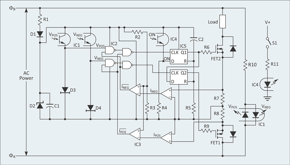
The circuit in Fig. 10 is nearly the same as the resistive TATTOO with addition of IC2 (a quad NAND gate), IC3 (a quad op-amp), shunts R7 and R8, R2 and R3 (a voltage divider) and R5 and C2 (a power-on reset circuit.). The logic signals INEG and IPOS (and their logic inverses) are developed once the current starts flowing.
 |
|
| Figure 10. | A reactive load requires addition of the quad NAND gate: IC2: quad op-amp IC3: voltage dividers R7 and R8: R2 and R3: and R5 and C2: and power-on reset circuit. |
At the start of the ON pulse, the circuit operates as in the resistive TATTOO circuit. This is because IPOS and INEG are zero, enabling (via the NAND gates) the VPOS and VNEG signals to the flip-flop clock inputs as it did in the resistive TATTOO circuit. Once the current starts flowing through the shunt resistors, the op-amps develop the logic signals INEG and IPOS and their logic inverses. When these signals are developed, they gate off the VPOS and VNEG signals and only deliver the current gating signals to the flip-flop inputs. Therefore, the circuit now will turn off at the current zero crossings and ignore the voltage zero crossings.
Because the current signals depend on the value of the load current, it is expected that the shunts will be appropriately sized for several ranges of current. Of course, other current measurement devices can be used in place of the shunts if desired (Hall Effect devices, for example). If the current is insufficient to operate with the shunts, the circuit will default automatically to the normal mode (voltage mode).
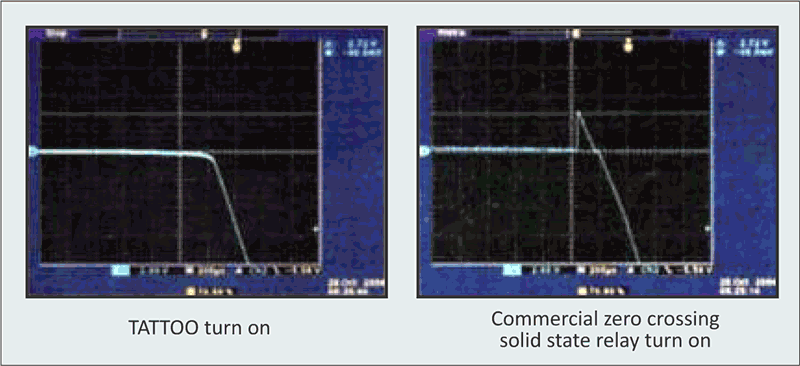
As stated before, some present commercial SSRs have a window of voltage that yields a fairly close operation to the zero-voltage crossing point but may not be acceptable for higher current operations or high frequencies. Fig. 11 shows the operation of a general commercial SSR with ZVS compared to TATTOO. The first oscilloscope plot shows an expanded view of the load current (60-Hz, 115-Vac supply) being applied to a load using the TATTOO circuit. The second plot shows the same load being turned on but using a commercial SSR with ZVS instead.
 |
|
| Figure 11. | Other products claim to operate at the zero-voltage crossing, but may not be as precise as the TATTOO circuit. |
The plot of the waveform for the commercial ZVS SSR shows there is a jump in the positive direction of the load current before the SSR applies voltage for the first negative cycle. Although this is a small deviation from the zero crossing (a little more than 2.5 V), the TATTOO waveform shown in the adjacent plot proves to be much closer to 0 V during the turn-on operation. The actual published data for the commercial SSR lists a maximum of 15 V for the zero-voltage window. For the TATTOO turn on, there is no step in the positive direction and no sudden change in the current. This can be important for EMI considerations, especially with a high frequency of the AC supply and for high load currents.
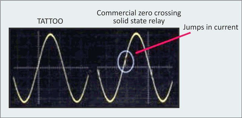
Fig. 12 shows the waveforms of load current when the supply frequency is raised to 2,000 Hz. The two plots compare the current waveforms of a TATTOO SSR versus a commercial ZVS SSR.
 |
|
| Figure 12. | An AC waveform at 2 kHz during normal operation is smoother with the TATTOO-based circuit. |
The TATTOO circuit can easily be modified to work over a wide range of power frequencies and voltages. A multi-phase TATTOO also is an easy modification by combining several TATTOO circuits (one for each phase). In the event a number of loads are to be switched from the same phase, the components common to that phase circuit need not be repeated. Therefore, the “POS” and “NEG” signal circuit and the floating VCC circuit need not be repeated, which will save components.
References
- SCR Manual, Sixth Edition, General Electric.
- Patent 7,196,435 B2 Handles Just Purely Resistive Loads by Turning the Load On at Zero-Voltage Crossing and Turns It off Also at Zero-Voltage Crossing.
- Patent 7,196,436 B2 Handles Reactive Loads in General by Turning the Load On at Zero-Voltage Crossing but Turns the Load Off at Zero-Current Crossing.
