This article is part of EDN’s Hot Technologies: Looking ahead to 2014 feature, where EDN editors examine some of the hot trends and technologies in 2013 that promise to shape technology news in 2014 and beyond.
The Internet of Things (IoT) conjures images of billions of smart devices, but just above these emerging IoT endpoints lies a critical layer providing data aggregation, analysis, and control. For this gateway layer and the endpoints below, embedded systems face challenges in performance and functionality to serve more sophisticated requirements for data collection and processing, as well as embedded vision, sensor fusion, and security, among others. Designers are facing these challenges head on and will make significant inroads in 2014.
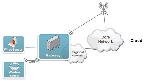
Platform solutions such as the "One Box" platform co-developed by Freescale Semiconductor, ARM, and Oracle illustrate the trend toward more comprehensive approaches for addressing IoT gateways between smart endpoints and cloud-based big data applications (Figure 1). "One Box" combines Freescale MCUs with Oracle Java and ARM Sensinode connectivity software to provide a reference platform for IoT gateways.
 |
|
| Figure 1. | In the Internet of Things, gateways serve multiple functions in handling signal processing, communications, control, and security between endpoints and the cloud. |
In an ideal world, an MCU targeting this gateway layer would combine multiple 32-bit high-performance cores; on-chip memory including NVM and SRAM partitions; parallel DSP pipeline; LCD controller; hardware-based security with root-of-trust; and multi-protocol radio transceivers -- all featuring ultra-low power operation for battery-operated target systems. Of course, the cost-benefit of such an idealized MCU would likely not hit the sweet spot of price-performance for these systems. Indeed, the very broad requirements for these systems argue against a tour de force of MCU integration. For example, a universal IoT controller would likely face a complex radio environment including not only WiFi (and eventually LTE/LTE-Advanced) on the cloud side but an alphabet-soup of data communications standards from ANT+ to ZigBee.
MCU makers are responding to the need for greater intelligence in the IoT periphery with highly integrated and even reconfigurable 32-bit-based multicore architectures that merge traditional features and capabilities of deeply embedded systems with higher-end application processors. What's unique about these devices is that their application target remains broader embedded computing -- even as a broad array of innovative special-purpose MCUs appear, targeting specific applications including motor control, smart meters, security, and more.
IC manufacturers wrapped up 2013 with a flurry of announcements that set the stage for general-purpose MCUs that push added intelligence and connectivity into endpoints and endpoint control/aggregation layers. Look closely, and you'll find that in most cases, the new devices reach impressive levels of integration while targeting embedded designers' needs for improved code density, greater horsepower, and DSP-oriented features meant to serve the growing need for signal processing in the periphery. The examples below represent only a few examples of these high-performance MCUs, but showcase some of the predominant approaches for addressing this emerging market.
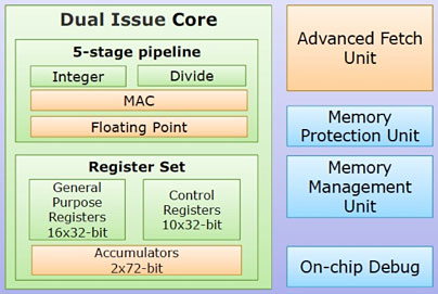
Renesas built in support for signal-processing applications in its new 32-bit RXv2 core with the addition of two 72-bit accumulators and a single-cycle MAC instruction with 32 × 32 multiply. In addition, Renesas used a combination of architectural features and 40nm process technology to achieve a 25% performance improvement with a 40% power reduction compared to the earlier RXv1 core. Underlying the performance boost, Renesas built in a dual-issue pipeline and AFU (Advanced Fetch Unit), which optimizes wait states and serves as an instruction cache for flash. The resulting architecture delivers 4.0 Coremark/MHz or 2.0 DMIPS/MHz, with a maximum frequency of 300MHz in 40nm.
 |
|
| Figure 2. | The Renesas RXv2 features a dual-issue pipeline, an advanced fetch unit for optimized flash access, and DSP features for enhanced performance. |
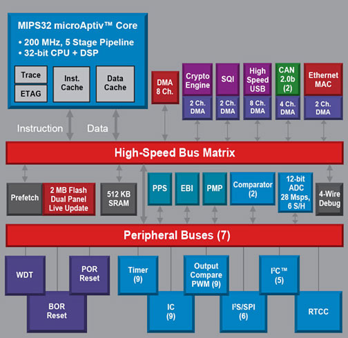
Microchip Technology built its PIC32MZ MCU family around the 32-bit Imagination Technologies MIPS 200MHz microAptiv core, integrating the core with large memory stores and a broad range of peripherals for data acquisition, connectivity, and security. The microAptive DSP-enhanced core brings 159 DSP instructions, which in combination with the integrated 28 Msps 12-bit ADC delivers a significant signal-processing platform. For connectivity, the family boasts a 10/100 Ethernet MAC, Hi-Speed USB MAC and PHY, dual CAN ports, SQI, and multiple UART, SPI, and I2C modules, among others. Security features include an integrated crypto engine and access control for memory and peripherals, which provides needed security to complement the family's two separate protected flash banks for live update support. Along with its support for the earlier MIPS32 instruction set, the microAptive core features the microMIPS instruction set architecture. The more efficient microMIPS core enables the PIC32MZ family to achieve 30% code density improvement compared to earlier 32-bit PIC MCUs, while delivering 3.28 CoreMarks/MHz and 330 DMIPS.
 |
|
| Figure 3. | The Microchip Technology PIC32MZ MCU family combines the advanced microAptive core with a broad range of peripherals needed to support the diverse functionality requirements of IoT gateways. |
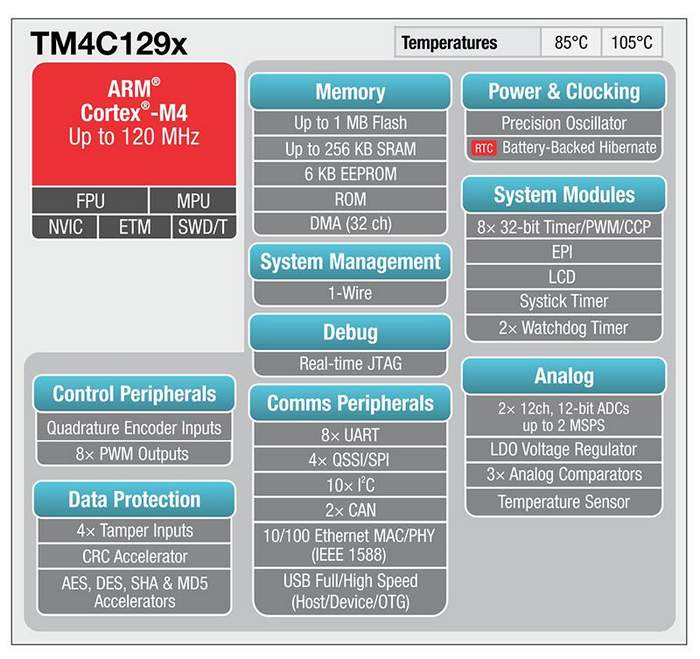
The Texas Instruments Tiva C Series TM4C129x offers the industry's first ARM Cortex-M4-based MCU with integrated Ethernet MAC+PHY. Superset configurations combine the Ethernet MAC+PHY with large flash and SRAM partitions, two 12-bit ADCs, and multiple additional connectivity peripherals including CAN, High-Speed USB, UARTs, SPI, I2C, among others. In addition, the MCUs include QEI (Quadrature Encoder Input) ports, PWM ports and an LCD controller. For security, the devices integrate dedicated crypto engines and feature four dedicated tamper ports designed to support security policies such as memory erase if unauthorized access occurs.
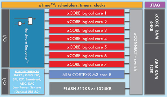
For its xCORE-XA (eXtended Architecture) device family, XMOS integrated a Silicon Laboratories low-energy implementation of the ARM Cortex-M3 with its own xCORE cores and low-power peripheral and analog blocks. Designed for high-performance signal-processing and control applications, the xCORE-XA allows engineers to configure one or more xCORE cores as soft peripherals addressing more specialized requirements for processing and connectivity.
 |
|
| Figure 5. | XMOS combined a low-energy ARM Cortex-M3 with its xCORE cores to provide a configurable multicore MCU designed to support high-performance requirements while retaining support for legacy control code. |
The examples of this trend continue throughout the industry. The latest HS34 and HS36 processor cores in its DesignWare ARC HS Processor family feature a 10-stage pipeline, optional DSP features, and an extensive set of configurability options -- along with associated peripherals available with its DesignWare offering. NXP Semiconductors' LPC4370 MCU combines an ARM Cortex-M4 with a Cortex-M0 coprocessor for handling I/O and other tasks. Peripherals include an 80 Msps 12-bit ADC, High-Speed USB with integrated PHY, Ethernet, and LCD controller. The Atmel SAMA5D3x family combines an ARM Cortex-A5 in configurations that variously integrate blocks for gigabit Ethernet, dual Ethernet, dual CAN, LIN, SPI, USB, LCD controller, and security options such as secure boot loader and crypto accelerators. The 180MHz STM32F429/STM32F439 MCU series from STMicroelectronics combines an ARM Cortex-M4 with a variety of blocks including an LCD controller and graphics accelerator to support rich user interfaces in embedded designs for IoT endpoints and gateways.
