David Hunter, Analog Devices
Analog Dialogue
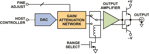
In the past, the most difficult part of an arbitrary waveform generator was designing the output stage. Typical signal generators offer output ranges from 25 mV to 5 V. To drive a 50-Ω load, traditional designs used high-performance discrete devices, a large number of integrated devices in parallel, or an expensive ASIC, with designers spending countless hours to create a stable, high-performance output stage with a wide programmable range (Figure 1). Now, advancements in technology have produced amplifiers that can drive these loads, reducing output stage complexity while decreasing cost and time to market.
 |
|
| Figure 1. | A typical signal generator model. |
When using general-purpose signal generators, a frequency is entered, a button is pressed, and the instrument produces a new frequency. Next, the desired output power is entered, and another button is pressed. Relays click as they switch internal networks to adjust the output level. This discontinuous operation is required to compensate for the lack of a wide programmable range. This article proposes a new architecture that also solves this half of the problem with the output stage design.
 |
|
| Figure 2. | The smaller, simpler, signal generator output stage. |
The two key components that solve this front-end design challenge are: a high-performance output stage that provides high speed, high voltage, and high output current; and a variable-gain amplifier (VGA) with continuous linear-in-dB tuning. This design targets 20-MHz performance, with 22.4-V amplitude (+39 dBm) into a 50-Ω load (Figure 1).
New Compact Output Stage
The initial signal may come from a digital-to-analog converter (DAC) for a complex waveform, or from a direct-digital synthesis (DDS) device for sine-wave generation. In either case, its specifications and power adjustment capabilities may not be ideal. The first requirement is to provide attenuation or gain using a VGA. The gain provided by many VGAs is limited, however, and is seldom enough to be useful for this application.
If the output of the VGA can be set to a target level, then no matter what the input is, the output can be forced to a known amplitude. For example, if the desired output amplitude is 2 V, and the power output stage has a gain of 10, then the output amplitude of the VGA should be regulated to 0.2 V. When the output stage is correctly designed, the output amplitude is ultimately set by the output of the VGA. Unfortunately, most VGAs become the bottleneck due to their limited programmable range.
A typical, high-quality signal generator offers an output amplitude range of 25 mV to 5 V. This 46-dB adjustable range exceeds the capabilities of most commercially available VGAs. The AD8330 [1] was the first VGA to achieve a 50-dB range, but the bar was raised further with the AD8338 [2], a new low-power VGA with an 80-dB programmable range. Under ideal conditions, the output amplitude of a classic signal generator could then range from 0.5 mV to 5 V, without the use of relays or switched networks. The full range would be continuously adjustable, free of the discontinuities associated with switches and relays. In addition, eliminating the relays increases instrument lifetime and system reliability.
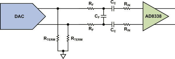
Modern DACs and DDS devices often have differential outputs, requiring designers to use a transformer, lose half of the signal with a single-ended connection, or add a differential-to-single-ended converter. The AD8338 provides a natural fit, having a fully differential interface, as shown in Figure 3. For a sine-wave application, the DAC would be replaced with a DDS.
 |
|
| Figure 3. | Example of a network that interfaces a DAC to the AD8338. |
A major feature of the AD8338 is the flexible input stage. As an input-VGA, it manipulates the input currents using the “H-amp” topology invented by ADI Fellow Barrie Gilbert. This design uses feedback to balance the input currents while maintaining the internal nodes at 1.5 V. Under normal conditions, using the 500-Ω input resistors, the maximum 1.5-V input signal produces a 3-mA current. If the input amplitude were larger, say 15 V, a larger resistor would be connected to the “direct” input pins. This resistor is sized such that the same 3-mA current is obtained:
| (1) |
The single-ended 15-V signal would output 1.141 V differentially. In this case, at minimum gain, the AD8338 would provide 28.4-dB attenuation, so the maximum possible gain is +51.6 dB. As a low-power part, it has a 1.5-V typical output swing into a 1-kΩ load.
The power of the input VGA is that its total gain range can be located around different set points. First, determine the output level required to produce the signal generator’s maximum output. Many commercial generators only provide a 250 mW rms (+24 dBm) maximum output power into a 50-Ω load (sine wave). This is not enough to cover applications that need more output power, such as testing high-output HF amplifiers or ultrasound pulse generation, for example.
Advances in current-feedback amplifier (CFA) technology mean that this no longer has to be a problem. The ADA4870 [3] CFA can drive 1 A at 17 V on ±20-V supplies. For sine waves, it can output frequencies up to 23 MHz at full load, making it an ideal front-end driver for the next generation of general-purpose arbitrary waveform/signal generators.
For 50-Ω systems that are sensitive to reflections, the ADA4870 requires some passive devices to match the source impedance to the 50-Ω load: a resistive pad and a 1.5:1 RF autotransformer. Allowing 1 V of margin, 8-W peak power is obtained when the effective amplifier loading is 16 Ω. Alternatively, if reflections are not a concern, the resistive pad can be eliminated, and the autotransformer can be replaced with one with a 0.77:1 ratio. Without the resistive padding the output power increases to 16-W peak (28.3-V amplitude).
 |
|
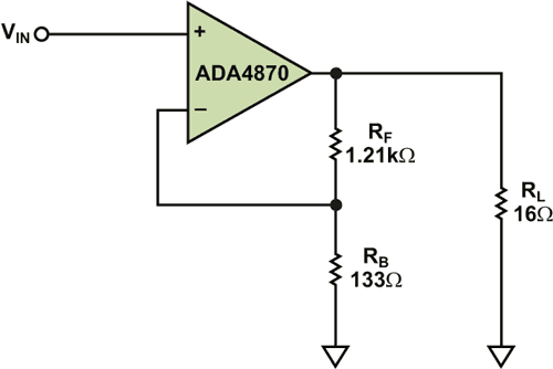
| Figure 4. | The basic connection for the ADA4870 for driving 16 Ω, gain = 10. |
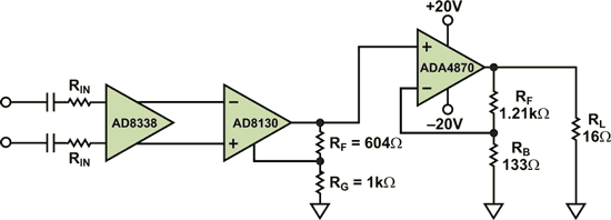
To optimize the output signal swing, the ADA4870 is configured for a gain of 10, so the required input amplitude is 1.6 V (Figure 4). The ADA4870 has a single-ended input, and the AD8338 has a differential output, so an AD8130 [4] differential- receive amplifier, with its 270-MHz gain-bandwidth product and 1090-V/µs slew rate, provides both the differential-to-single-ended conversion and the required gain. The AD8338’s output is constrained to ±1.0 V, so the AD8130 must provide an intermediate gain of 1.6 V/V. When combined, the three devices form a complete signal generator output stage (Figure 5).
 |
|
| Figure 5. | Signal generator output stage. |
Two final steps are required to complete the design: con- figuring the input network for maximum input signal plus antialiasing, and designing the output network for an impedance transformation.
