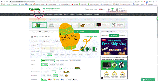
We are usually eager to see how the PCB we design shows after it is manufactured. Professional makers probably have various software to visualize their designs. But, novices and hobbyists are unlikely have access to those software and may be not clear about the software feature and how to use them.
Recently PCBWay has released a Free Online Gerber Viewer to visualize the Gerber files produced by a PCB CAD tool. The tool supports the Gerber RS-274X format, which is an industry-standard image description format for PCBs. PCBWay's tool will bring about images for each layer with combined images for the top and bottom of the board. Apart from providing a guide as to the final facade of the PCB, including your selection of solder mask color, the tool also provides different analysis steps. It helps guarantee your design doesn't breach any Design for Manufacture (DFM) rules that might cause not being manufactured properly.
Step 1: Upload Your Gerber Files in PCBWay Gerber Viewer
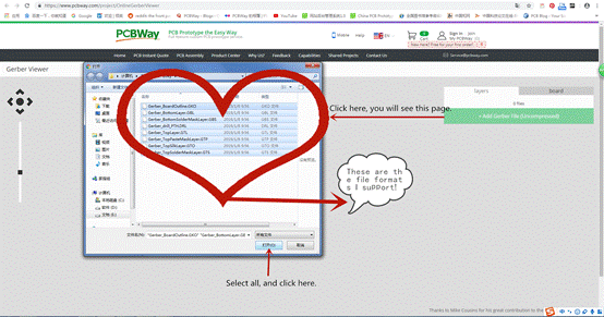
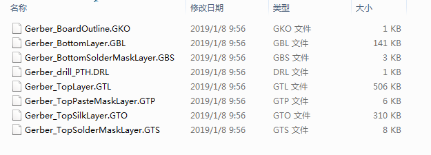
It’s recommend you directly go to https://www.pcbway.com/project/OnlineGerberViewer.html and upload the files there to view your whole design’s appearance. Also, if you try the Viewer from other software, it should be compatible with the files generated by any software. Tutorials links for taking out Gerber files from Altium, Eagle, Diptrace and KiCad have been given on Gerber Viewer page.
Step 2: Viewing Your PCB Designs on PCBWay Gerber Viewer
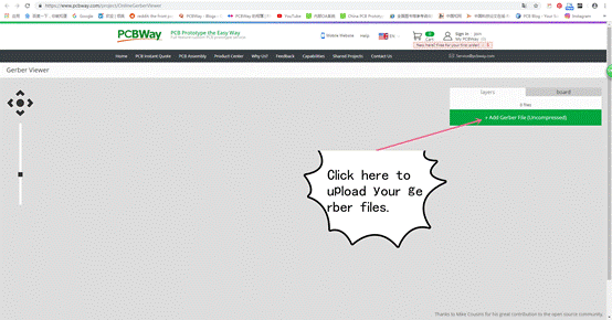
This picture illustrates how to upload your files to PCBWay Gerber Viewer. Just click on ‘+ Add Gerber File (Uncompressed)’ button on this page to upload your files.
 |
 |
Step 3: PCBWay Gerber Viewer Tool User Interface
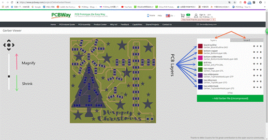
The Gerber Viewer is greatly user-friendly because you can find many options and settings. A novice PCB designer who lacks knowledge about different layers of PCB can also view and understand the importance of different Gerber files. Certainly, various colors for solder mask, silkscreen and copper fill are waiting for you to choose. PCBWay Gerber Viewer will produce it as images including a top side and a bottom side photo view. Meanwhile, PCBWay runs a simple Design For Manufacture (DFM) check. This will show you the board size, hole and track sizes and clearances of the different PCB objects such as tracks and pads.
Step 4: See the Top or Bottom Layer of PCB
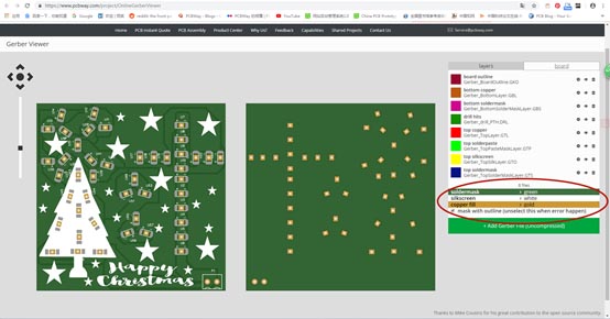
This photo shows the top and bottom layers of PCB on the board frame. You can also change settings of each layer.
There are more amazing options, just upload your Gerber file and check them out in PCBWay Gerber Viewer.
PCBWay provides first-class flexible PCBs and PCB Assembly. We embrace all professionals, makers, designers, novices and hobbyists to try and enjoy our services!
