Recently, JLCPCB will not charge color fee on PCB any more, that is, $2 for any color is reliable on JLCPCB. Before, other colors need to charge extra fee, like red color, extra $5 and black color, extra $10. But now no color fee any more on JLCPCB: https://jlcpcb.com.
There are a number of stages involved in the design and manufacturing of PCBs. You must have a clear idea of these stages in order to produce high quality circuit boards. The layout and design of your PCB are integral elements which have a large impact on that way your circuit board operates.
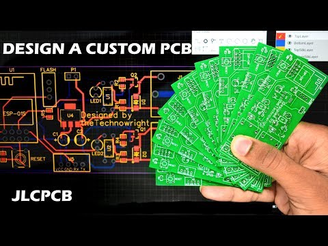
Equipment Required For PCB Design
If you wish to design PCBs for commercial use, there are a number of CAD (Computer Aided Design) Packages available which can help reduce the complexity. Simple PCB designing software is available, but you can also purchase top end products in order to get more facilities to aid your design. Simulations are also becoming a requirement with the increase in the speeds of digital boards, and higher frequency operating radio designs.
Circuit Schematic Capture
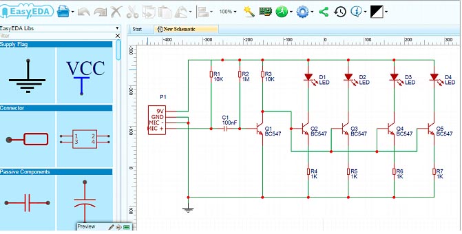
The first stage of development involves capturing the schematic for the circuit. This can be done using a schematic capture tool. In some cases, simulations of the circuit may be taken at this stage. Some packages have the ability to interface to simulation packages. For applications involving Radio Frequency (RF circuit design) simulation will help to optimize the final circuit without building a prototype. Once the schematic capture is complete, the design is contained within a file and is now called a ‘netlist’. A netlist contains all the necessary interconnectivity information; a list of the electronic components and the nodes they are connected to.
Initial PCB Component Placement
Before you start with design and layout, try to estimate the number of layers and components, their location on the board, necessary space requirements etc. Then try to form a more detailed component layout for the PCB design. Try to take aspects such as the proximity of devices that may intercommunicate and other necessary information regarding RF considerations into account.
Make sure that you have all the necessary information regarding all the components you will be using in your design. This includes footprints, drilling information etc. Within the PCB layout design system a library will be built up with all the devices used listed. This can help you organize all the components and find previously used components easily.
Routing the Connections
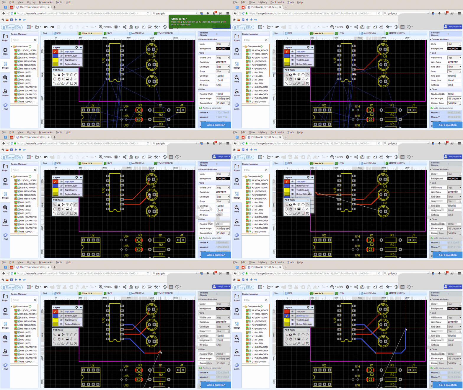
The next stage involves the routing of the connections between components. The routing is done through the netlist from the schematic. A number of layers and via holes may be required in the design. One layer is used as a ground plane while other is used as a power place. This enables low source resistance connections to be made for power, and helps reduce noise levels. Routing can be difficult as thousands of components may be required at times.
Required PCB Files
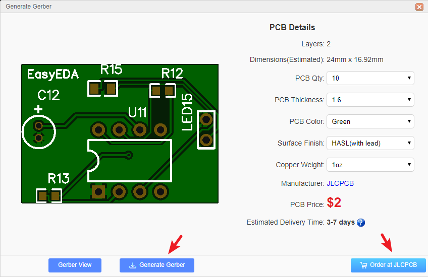
The Gerber file gives an outline of the PCB layout through photo plots. Along with Gerber files, drill information, screen print and photo-resist information may also be required. Drilling of the PCB may be expensive. Hills may be required for fixing or for conventional components. You can however reduce the costs by reducing the hole sizes as much as possible. The drill will therefore need less changing and will be less time-consuming as well.
PCB Testing
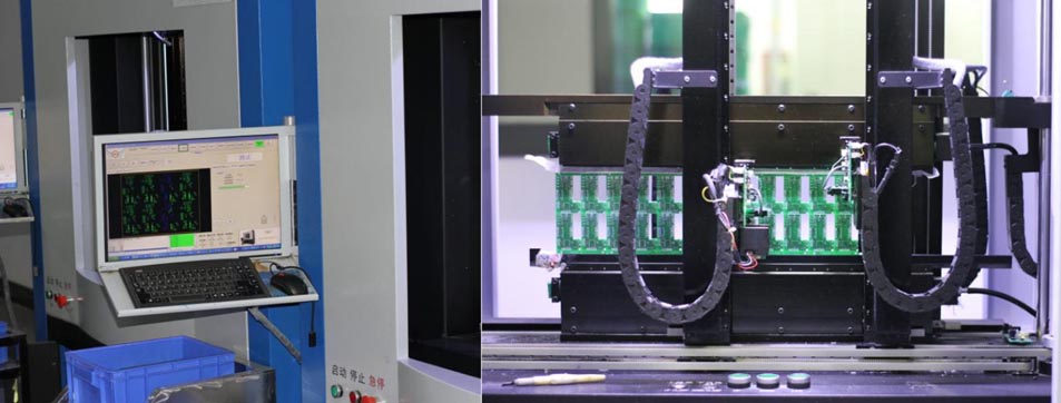
After the fabrication process, the board moves on to the ‘testing’ stage. Here the PCB is validated to make sure it meets the required specifications. After testing, the PCB can then move on towards the product development stage.
Why Use Prototyping?
There are a number of reasons why prototyping is a better option for you to undertake. For one it saves your time and money. It is excellent for testing new innovations before putting them into large scale development stages, this way you can easily test the risk of failure beforehand. This will help you to also gather more accurate requirements before you begin your project to see any shortcomings. This also helps you to recognize the technical problems that may arise in your design so you may solve them and hence make your design more accurate. You can also try to use a number of approaches on your design and test it however you wish.
Conclusion
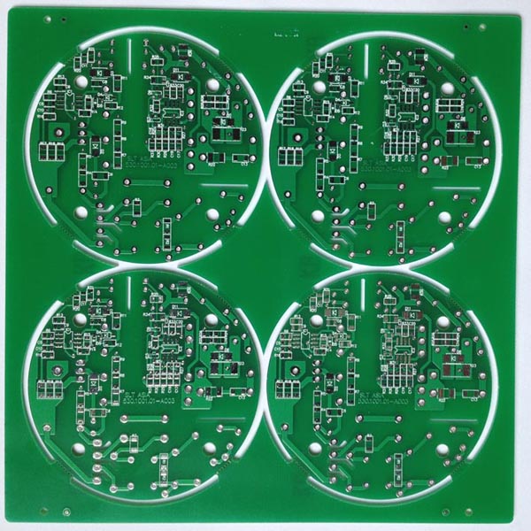
The information provided in the design files will be used in many stages of the manufacturing process. They contain necessary information for the pick and place program, in the manufacturing of solder mask, for the testing of the PCB etc. Therefore, we conclude that the PCB design is not limited to the basic design of the board, but is rather a crucial element of the entire PCB fabrication process.
