The flyback topology is a versatile, widely used, switched-mode power-supply design with some interesting characteristics that brings performance and BOM advantages to many applications.
The flyback design is a switched-mode power supply (SMPS) that’s been used for 70+ years and still going strong. This supply – also called a power converter – has two distinct operating phases, with power from the input side transferred to the output side only when the primary-side switch is off and its current flow is zero or close to it. The core of the flyback design has a fairly short and low-cost bill of materials (BOM): input capacitor, primary-side MOSFET switch, output (secondary)-side rectifier diode, and an output capacitor. In addition, there’s the flyback transformer itself (of course, as with any design, the final schematic is more complicated).
The flyback design was developed the 1930s and 1940s, and highly refined in the 1950s with the introduction of commercial television. In some ways, it precedes our modern concept of the nonlinear switching supply.
In its earlier roles, the flyback converter provided the high voltages needed for the CRT and the other vacuum tubes, which were the “active” electronics before transistors and ICs. As a result of this huge market, it was engineered and optimized for low cost, high reliability, safety, and manufacturability. The flyback design and characteristics are well-suited for low-to-medium power range applications between 100 to 250 W.
Flyback Converter Basics
Unlike a non-flyback design where the transformer is used only for voltage step-up or step-down, the flyback transformer is also used as an inductor, a magnetic energy-storage device. This transformer has additional windings (critical to the flyback operation) beyond being a basic two-winding (primary/secondary) transformer. The turns-ratio of the transformer serves two roles: it sets the output versus input voltage ratio, and it provides galvanic (ohmic) isolation. By using additional windings, the flyback design can simultaneously provide multiple outputs.
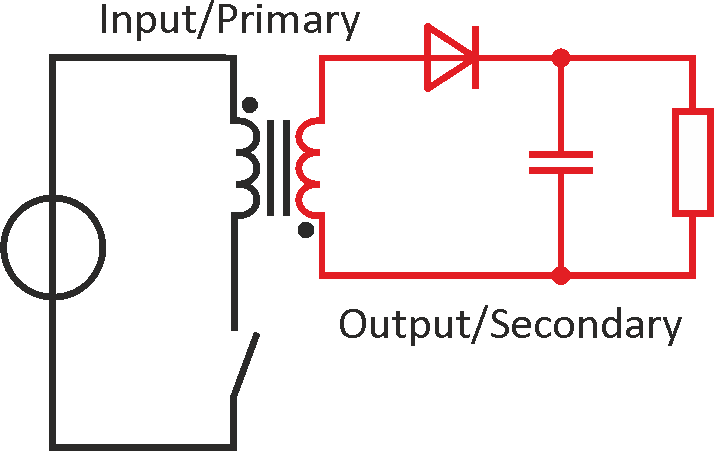
In the basic flyback cycle, closing the primary-side switch increases the primary current and magnetic flux in the transformer/inductor as the primary-side circuit is supplied by the source (Fig. 1). The voltage in the secondary-side winding is negative due to the relative relationship between primary and secondary windings. Therefore, the diode is reverse-biased and blocks current flow and the secondary-side capacitor supplies the current to the load during operating phase.
 |
||
| Figure 1. | In the first cycle of flyback-converter operation, the primary-side switch is closed, thus increasing the primary current and transformer/ inductor magnetic flux. (Source: Wikipedia) |
|
The switch is opened on the next phase of the cycle (Fig. 2), so the primary-side current goes to zero and the magnetic flux collapses. Now the secondary-side voltage goes positive, the diode is forward-biased, and current flows from the transformer secondary side to the capacitor, thus replenishing the capacitor.
 |
||
| Figure 2. | In the second cycle of flyback-converter operation, the primary-side switch is opened and current flows from the transformer secondary side to the capacitor. (Source: Wikipedia) |
|
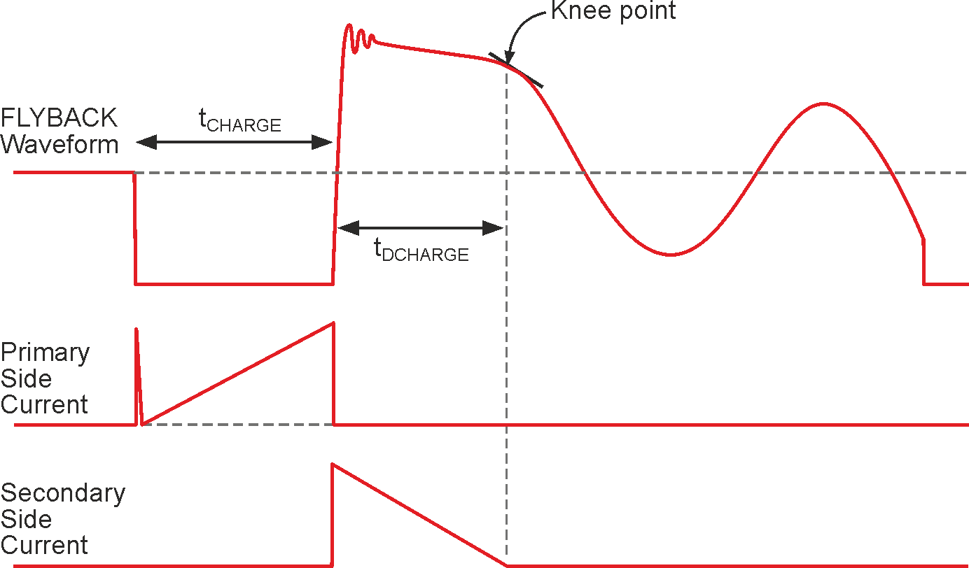
In a flyback design, the output capacitor is similar to a bucket that’s either being filled (recharged) or emptied (supplying the load), but it never undergoes both at the same time. The resultant output ripple must be filtered by the capacitor, which is never allowed to drain down to zero charge. The “flyback” name is due to the sudden stop/stop, on/off action of the MOSFET switch, with a waveform that looks like a sudden reversal of current flow (Fig. 3).
 |
||
| Figure 3. | The basic waveshape of the flyback topology shows the sudden reversal and transitions for primary and secondary-side currents. (Source: Wikipedia) |
|
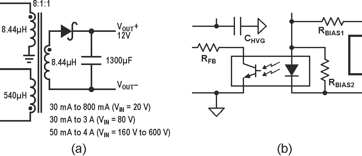
Regulation of the output is achieved by adjusting the on/off duty cycle of the primary-side switch. Some designs also adjust frequency of the switching action (faster switching results in closer tracking of the output to the desired output value. This feedback with required input-output isolation is provided either via a special winding on the transformer (the traditional and historical approach) (Fig. 4a) or via an optocoupler (Fig. 4b).
 |
||
| Figure 4. | The traditional flyback design uses a transformer/inductor with at least two primary windings and one secondary winding (a). Some flyback designs use an optocoupler to provide the isolated feedback equivalent to the second primary-side winding (b). (Sources: Analog Devices and Texas Instruments) |
|
Operating Modes
Flybacks (and other many other converter types) can be designed to operate in one of two modes. In discontinuous conduction mode (DCM), the transformer is allowed to completely demagnetize during each switching cycle. Usually, this is done with a fixed switching frequency and modulation of the peak current to meet the load requirements. In continuous conduction mode (CCM), the current is always flowing in the transformer during each switching cycle. Therefore, some residual energy is always present in the transformer, because each switching cycle begins before the current is completely depleted.
With DCM, there are no reverse-recovery losses in the output rectifier since its current goes down to zero during every switching cycle. The required primary-side inductance value is low and needs only a smaller transformer. Analytically, the DCM design is inherently more stable, since there’s no zero in the right-half-plane zero of its transfer function. However, DCM has very large ripple currents and thus requires larger filters.
In contrast, CCM has small ripple and RMS currents. These lower currents also lower the conduction and turn-off losses, while lower peak currents allow for smaller filter components. But the CCM disadvantage is that it has a zero in the right-half-plane of the transfer function, which will limit the bandwidth of the control loop and its dynamic response. CCM also requires a larger inductance and thus a larger magnetic component.
Improving the Flyback Converter
As with any power-supply design, certain variations and enhancements can turn a good supply into a very good one. In DCM, there’s a dead time or resonant “ring” where neither the diode nor the MOSFET is conducting, created by interaction between the primary inductance of the transformer and the parasitic capacitance at the switch node. A quasi-resonant (QR) design adjusts the peak current and switching frequency so that the MOSFET turns on at the first “valley” of this resonant ringing and minimizes losses.
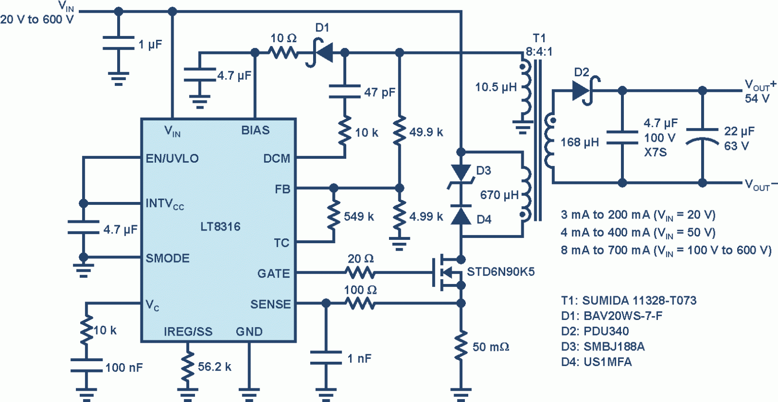
Modern IC controllers minimize many of the inevitable challenges of designing a complete flyback supply while enhancing performance. For example, Analog Devices’ LT8316 is a transformer-based, 20- to 600-V input flyback controller that can directly support loads up to 100 W (Fig. 5), supporting a wide span of output voltages.
 |
||
| Figure 5. | A complete 100 W isolated flyback converter from a 20 V to 600 V input. | |
The datasheet eases selection and identification of the flyback transformer by proving a table of common input/output voltage and current pairings matched to vendor names and models of standard available transformers. The result: creating a good flyback design is now a much easier project.
Conclusion
When selecting a power-supply/converter topology, there are many legitimate possibilities to consider, each with a unique set of features as well as positive and negative characteristics. These must be weighed against the system priorities and their technical performance and dollar costs. The flyback approach is a viable contender in applications under several hundred watts at voltages from single digits to kilovolts, and it’s especially attractive when multiple dc outputs and input/output isolation are required.
