Jeff Sorensen
EDN
2019 marks the 100th anniversary of the Greinacher voltage multiplier, invented by Swiss physicist Heinrich Greinacher in 1919. In 1932, Douglas Cockcroft and Ernest Walton used this basic circuit to power a particle accelerator, the first “atom smasher,” and eventually helped earn them the Nobel Prize in Physics in 1951. For this reason, it is most often referred to as the Cockcroft-Walton multiplier.
 |
||
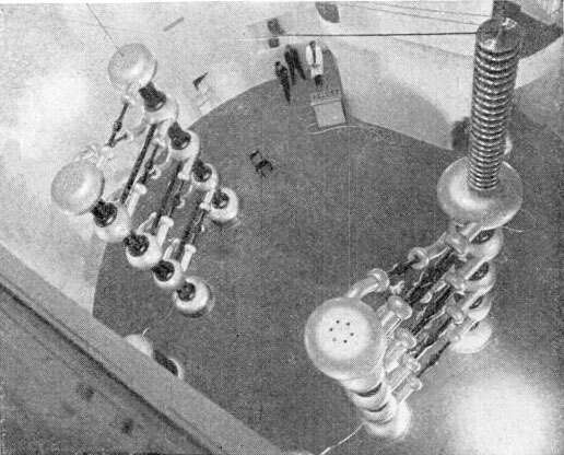
| Figure 1. | This Cockcroft-Walton full wave multiplier is shown at the Kaiser Wilhelm Institute in 1937. 3 MV could be generated by two 4-stage multipliers. Note the three people standing in the background. |
|
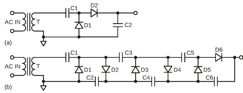
The key to this circuit is using a number of switches and capacitors to boost a lower voltage to a higher one. The first circuits were used to convert a high voltage AC voltage to an even higher DC voltage (Figure 1). Most applications for capacitive voltage converters are now for DC to DC. By using cascaded diode/capacitor stages, very high voltages could be generated while still using diodes and capacitors with voltage ratings of the individual stages, since the components only see the voltage in its own stage. The basic circuit is shown in Figure 2a. In this circuit the capacitor C2 top plate is charged to Vp on the positive half cycles and the bottom plate of C2 is charged to –Vp on the negative halve cycles. This means the voltage on C2 equals 2Vp. Multiple stages are connected in series, therefore each increase the voltage by 2Vp. In Figure 2b, the output will be 6× the peak voltage at AC in. C1, C3, and C5 pass the AC voltage along and C2, C4, and C6 are stacked to store the charge relative to the ground of the stages. A full wave version of this can also be implemented, as in Fig. 1, so the voltage becomes twice the voltage of the half wave example shown.
 |
||
| Figure 2. | Single and multi-stage Greinacher multipliers. | |
So, you’re probably saying to yourself, “That’s great, but I’m not smashing any atoms in my project,” but you probably have a very similar circuit in your PC or thumb drive. It turns out flash memory needs a higher voltage than its 1.8 V supply for writing and erasing the memory, and to make it possible to operate without a separate power supply. So there is a voltage multiplier built into the memory IC itself just for this purpose. It not exactly the same but it is arguably very similar, and since it is working with DC instead of AC, it therefore has to make its own AC, so to speak.
By slightly rearranging the diodes and capacitors, it is possible to comprise a circuit known as the Dickson charge pump. The Dickson charge pump (Figure 3) was patented by John F. Dickson in the late 1970s. It is used primarily in EEPROM/flash memory ICs to generate the programming/rewrite voltages that are well beyond the voltage that is available otherwise.
 |
||
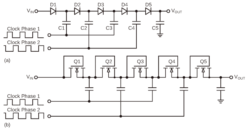
| Figure 3. | Dickson charge pumps use diodes and MOS-connected diodes. | |
The Dickson charge pump in Fig. 3a is very similar to the Greinacher doubler. A DC voltage is applied at VIN to diode D1’s anode. The voltage at the cathode of D1 will be one diode drop below VIN, and the anode of D2 will be another diode drop below that. When a VIN-level clock is applied to capacitor C1, the top of C1 will rise to the combined voltage of the output of D1 and the clock high level. This voltage then charges the second capacitor C2, already one diode below D1, through diode D2. The second capacitor now has the VIN voltage times two, minus the 2-diode voltage drops.
The multi-stage Dicksons in Fig. 3 uses a two-phase VIN-level clock that drive alternating capacitors, but a single stage could be used if a large output voltage boost is not required. Each stage is the clock level minus a diode drop higher than the previous stage, or

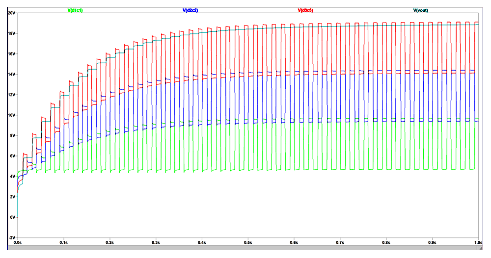
where N is the number of stages and VDIODE is the diode forward voltage drop. This does not account for the voltage loss (droop) due to the load current. Figure 4 shows a LTspice simulation output of a 3-stage Dickson with a VIN and clock level of 5 V. Each stage builds on the VIN voltage plus the voltage on each capacitor connected to the clocks. The top teal trace is the final DC level that is achieved. Note the phase relation between the boosted levels as well.
 |
||
| Figure 4. | This 3-stage Dickson charge pump shows the 4X voltage multiplication provided with this configuration. | |
MOS transistors connected as diodes are most often used in memory ICs, but Schottky diodes usually have lower forward voltages and therefore less voltage loss per stage. Many derivatives have been developed to improve the performance, particularly at lower voltage levels where the available VIN source voltage is low. This is particularly the case for memory devices running at 1.8 V or less.
These charge pump circuits could be termed “bucket brigade” charge pumps since each stage dumps a charge into the next stage.
The next type of charge pump could be called the “trapeze” charge pump, but is better known as the flying capacitor charge pump. These are very versatile because they can be used to boost, reduce, or change the polarity of the voltage it is providing. What makes them unique in their operation is that both ends of the capacitor are momentarily disconnected from the other circuitry at the same time, hence flying. Again, switches, almost always MOS transistors, are used to direct the current flow, but are used in pairs to connect the top and bottom of the capacitor to the charging source or the destination. It is important that there is dead time between states when switching the source and load switches so they are not closed at the same time. That could be a bad thing and cause current to flow where it is not wanted, therefore the need to “fly” between domains.
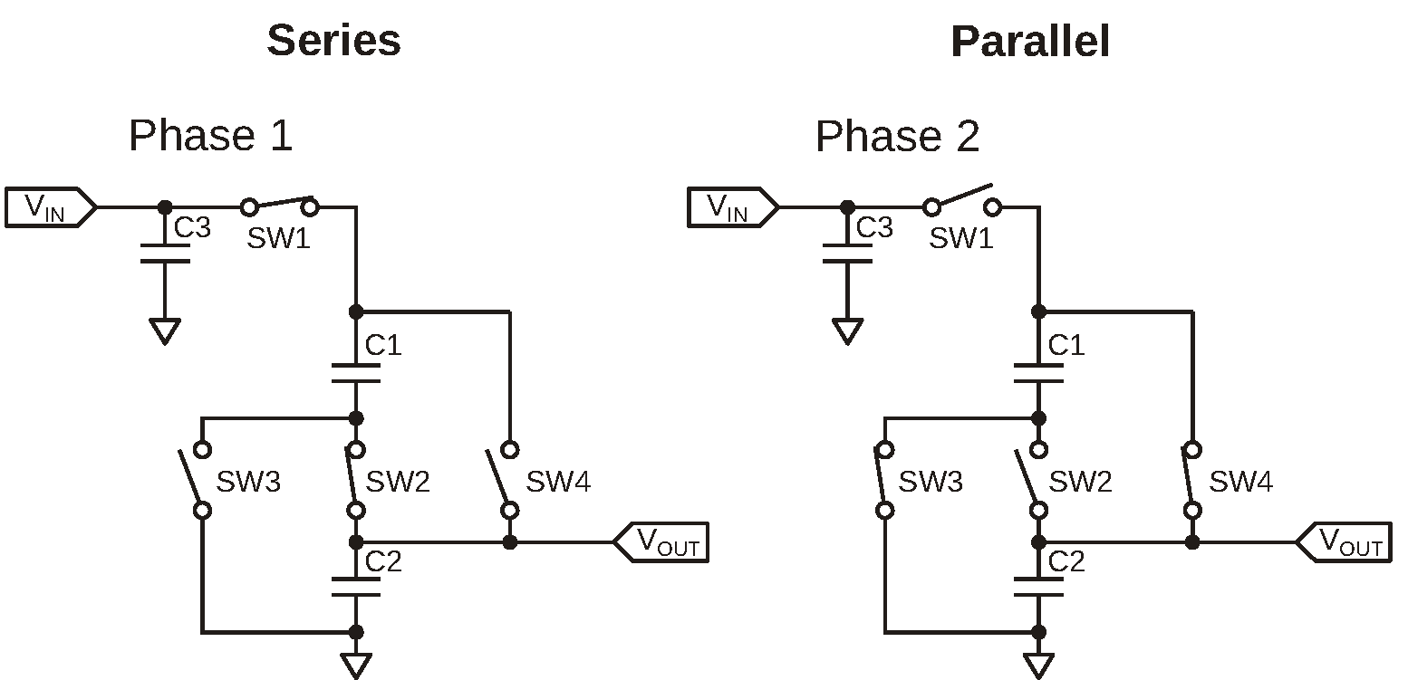
Figure 5 shows one example of a flying capacitor charge pump. The ports referenced VIN and VOUT have those functions in a voltage reduction mode of operation. The voltage at VIN is the voltage source and VOUT is the voltage being generated. In phase 1, the capacitors C1 and C2 are connected in series with switches SW1 and SW2, so each capacitor will be one half the voltage at VIN. In phase 2, the series switches are opened up and the parallel switches SW3 and SW4 are closed placing C1 and C2 in parallel and therefore have ½VIN as their combined voltage charge, so they have half the voltage, but twice the charge current available on the output due to the parallel capacitors.
 |
||
| Figure 5. | This is an example of a flying capacitor charge pump. | |
The main limiting factors are the resistances of the switches and the sizes of the capacitors. If low RDS(ON) (drain to source on resistance) switches are used, relatively high current can be supplied. The size of the capacitors can be reduced if the frequency of the switching is increased, but only up to a point. Eventually the switching losses become a factor with increasing frequency, so there are practical limits to how far the frequency can be increased for the switches. There are many commercially available products available that use this basic topology, which can supply from a few milliamps to amperes of current.
Multiple flying capacitors can be stacked and used to generate other division and multiplication factors as well. There are also negative output versions of this basic circuit that fly from a positive voltage to a negative voltage referenced to the ground pin. These are commonly used with operational amplifiers that require negative supplies and have low current requirements.
Another charge pump topology can also be used to generate a negative voltage from a positive one. This uses a diode-switched capacitor. All that is needed is a clock with an amplitude equal to the negative voltage that is desired.
In Figure 6, the input clock supplies the needed signal. On the positive edges the clock passes through C1 and D2 to ground. When the clock transitions to the low state, the AC coupled clock turns on D1 and charges C2 with a negative voltage. After a few cycles C2 is charged to the negative voltage equal to the clock’s amplitude, minus a diode drop. The amount of current available primarily depends on the impedance of the source, the frequency, and the size of the holding capacitor.
 |
||
| Figure 6. | In this voltage-inverting charge pump, the input clock supplies the needed signal. | |
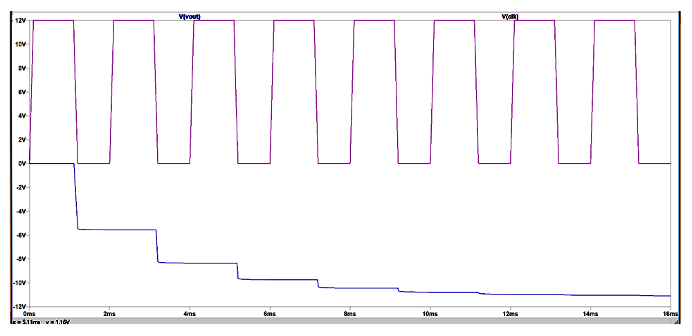
Figure 7 is a simulation using LTspice of the circuit in Fig. 6 and shows the clock (top violet trace) and output (bottom blue trace) for that circuit. If this resembles the operation of a Dickson charge pump, it isn’t a coincidence. It is essentially the same circuit, but generating a negative voltage on the capacitor and without the VIN positive bias that the traditional Dickson is built on. Otherwise it is identical.
 |
||
| Figure 7. | Here is the simulation output for the circuit in Figure 5. | |
Generally, charge pumps have been limited to lower voltages and currents, but the advancements of the MOS processes in terms of both voltage and power have made higher voltage and power charge pumps a reality. Large voltage conversion factors make charge pumps attractive choices instead of transformers in many power supply applications. Even when used to precondition a voltage for pulse-width modulated (PWM) regulators, they can help improve the overall efficiency compared to a single stage PWM converter. Since capacitors are relatively inexpensive and small, they can also reduce the cost and size of a voltage converter design. While the basic technology for capacitive voltage conversion has been around for 100 years, the semiconductor technologies needed to make them ubiquitous are only now catching up. Expect to see more of them in the future.