PCBA and PCB Manufacturing Introduction
The PCB Assembly Process and the PCB manufacturing process are often confused. The PCB manufacturing process of NEXTPCB involves designing and prototyping a printed circuit board whereas the PCB assembly process exclusively means the assembly of the PCB board from its components, attaching the various components to the circuit board.
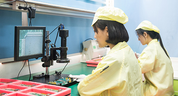
Requirements for Printed Circuit Board Assembly
For the assembly of printed circuit boards, you will require a set of components and equipment. These include:
- A Circuit Board:
You will need a primary circuit board on which you will assemble the components. - Electronic Components:
PCBs include a variety of complex electrical components including resistors, capacitors, diodes, transistors, and fuses. - Soldering Material:
A solder is a metal alloy made from tin and lead which is melted and then cooled to form a strong bond. - Soldering Equipment:
This will usually include a wave soldering machine and soldering station and the equipment for surface-mount and through-hole tech (whichever you’ll be making use of). - Equipment for Testing:
Testing is important to ensure that your PCB is reliable and ready for delivery.
Once you’ve got all your equipment and electrical components ready, you can proceed with the PCB assembly process. There are two types of technology you can use depending on the types of components you will be assembling i.e. Surface-Mount Technology and Thru-Hole Technology.
Surface-Mount Technology
SMT or Surface Mount Technology is the method through which smaller, sensitive components such as transistors and diodes are mounted directly onto the surface of the PCB instead of wiring. This type of technology is generally used with components known as Surface Mount Devices or SMD’s which are further of three types:
- Passive SMD’s (resistors, capacitors)
- IC’s (Integrated circuits)
- Transistors, diodes
Thru-Hole Technology
Through Hole (or thru-hole) Technology involves inserting the leads or wires of components into holes drilled into the PCB and plugging them. The extra wiring on the other end of the PCB board is soldered to pads. This type of technology is mainly used for through-hole components. These are two types of Thru-hole components i.e.
- Axial Lead Components – having lead running axially (in a straight line) through the component
- Radial Lead Components – having lead exiting from a common side of the component instead of the opposite ends
Difference between Surface-Mount Technology and Thru-Hole Technology
- THT is used for large components whereas SMT is used for smaller components and so is useful in building smaller-sized PCBs.
- THT components have lead wires which pass-through holes and are soldered to the other end whereas SMT components do not have leads and instead are mounted directly to the PCB.
- SMT assembly is usually done via automated technology as small-sized components are harder to place manually and so are ideal for high volume production. On the other hand, THT will require different types of equipment and generally involves larger, bulky components which can be placed manually.
- SMT is a lot more advanced as opposed to THT and is more commonly used in modern PCB assembly.
PCB Assembly Process
The PCB assembly process involves the application of solder paste, picking and placement of components, soldering of components, an inspection of the PCB board and testing. These are the general steps in the PCB assembly process that you will commonly find. The process we’ll be describing assumes that SMT components are being used.
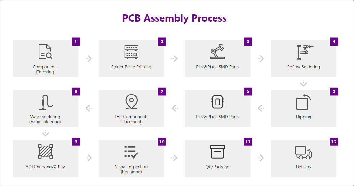
Application of Solder Paste
Solder paste is used in PCB manufacturing in order to connect surface mount components to the pads on the circuit board. Solder paste is applied to the board before the pick and place of components.
Solder paste is generally composed of a tin-lead alloy that is melted. A solder screen containing holes right where the solder pads are generated is placed on the board. Then, a runner moves along the screen depositing solder paste through those holes onto the board where required.
Picking and Placement of Components
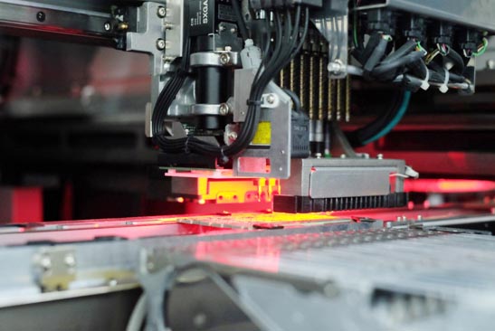
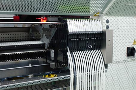
The next step involves the placement of components onto the printed circuit board. This process involves a pick-and-place machine also known as an SMT component placement system. It will essentially lift up the components off a reel or dispenser, rotates them to the right orientation, and places them onto the circuit board where required. The solder will help keep the components in place.
Soldering of Components
Once the components are placed onto the board, the next step involves soldering of the components. Soldering generally involves the joining of two or more items, in this case, the surface-mount component and circuit board, by melting solder which then cools to solidify and form a strong electrical bond.
There are two general types of soldering processes
- Reflow soldering – used for surface mount components. In this, the solder is applied and then subjected to controlled heating to form a solder joint.
- Wave soldering – used for thru-hole components. In this, the solder is not pre-applied rather the circuit board passes over a pan of molten solder.
Inspection of PCB Board
Once the components have been soldered onto the printed circuit boards, the board moves on to the inspection process. This process is typically automated rather than done manually, as it reduces the chances of error although it can be done manually too. Typical methods of inspection include visual inspection, automated optical inspection and automated x-ray inspection.
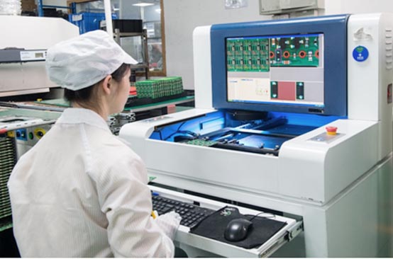
Testing
Testing is the final step in the PCB assembly process. Testing is essential to weed out any underlying errors that may have passed through inspection. Further, it allows you to see if the PCB design needs any changes.
Typical PCB testing methods include in-circuit testing, the flying probe test, burn-in testing, and functional testing. Any errors that are identified in the inspection or testing phase are sent via feedback so they can be immediately rectified.
Conclusion
Here the PCB assembly process has been rather simplified for you when in reality it is a very critical process. The right PCB manufacturing company will give due attention to every step along the way to ensure minimum defects or chances of error.
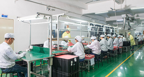
NextPCB – one of the best in the industry
NextPCB is a top-performing PCB company with its headquarters stationed in Shenzhen, China. With over 10 years of experience in the PCB manufacturing industry, it has acquired a reputation for manufacturing high-quality PCBs and quick delivery of products.
NextPCB offers PCB assembly and PCB manufacturing services along with prototyping, and testing, which vary from low-volume to high-volume production lines as required, making them a one-stop solution. We offer all types of PCB manufacturing ranging from rigid Rigid PCBs, Flexible PCB, metal core PCBs to Rigid-Flex PCBs using SMT, BGA, and Thru-Hole assembly to name a few. After production NextPCB offers a number of tests for quality inspection and testing including visual inspection, AOI, x-ray inspection, ICT, and functional testing. We are also IATF16949, ISO9001, ISO14001, UL, CQC, RoHS and REACH certified proving them to be highly reliable.

To top it off they also offer various payment and shipping methods. You can pay via PayPal, Bank Transfer, or Western and choose either DHL, FedEx, or Hong Kong Post for shipping.
Still, need help? Contact Us: support@nextpcb.com
Need a PCB or PCBA quote? Quote now
