This article describes a technique to compensate the DC voltage drift in the output of a directly-coupled AB-Class audio power amplifier.
The main benefit of a directly-coupled output is improved bass response. Since the design eliminates the DC-blocking capacitor, its low-frequency transfer characteristics are significantly improved.
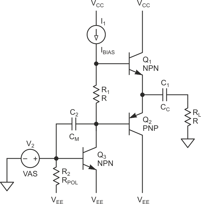
Figure 1 shows a capacitor coupled output, where the cut-off low frequency is determined by the load (typically 8 Ω) and the capacitor CC. In this example, the capacitor CC is blocking any DC offset that could appear in the output.
 |
|
| Figure 1. | The capacitor-coupled output’s cut-off low frequency is determined by the load, the capacitor CC, and the output network. |
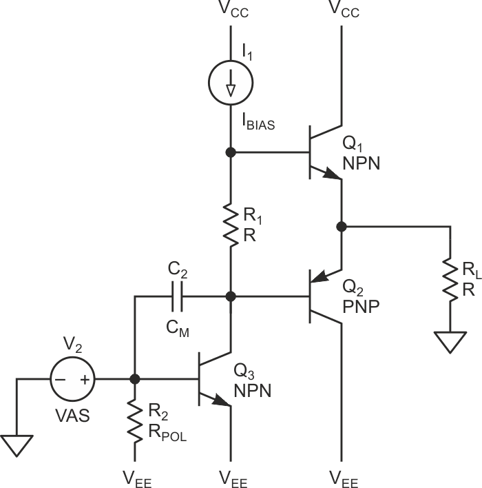
This is not the situation in the directly-coupled counterpart (Figure 2). Its lower cut-off frequency is not limited by the output, so any fluctuation in the previous stages will cause the DC value to fluctuate, resulting in a DC current flow through the load (speaker). Besides degrading the dynamic range and THD of the amplifier, this is also the reason why sometimes we hear a “click” noise when turning on or off a discrete audio amp.
 |
|
| Figure 2. | The directly-coupled output’s lower cut-off frequency is not limited by the output. |
To correct this problem, we will first perform a deep analysis to understand the reason behind the DC offset of a discrete bipolar junction transistor (BJT) audio amplifier. Next, we will devise a method to eliminate or at least mitigate this issue.
Let’s begin by creating a simple model of the amplifier, including the main stages (Figure 3).
 |
|
| Figure 3. | Here is a simple model of the amplifier. |
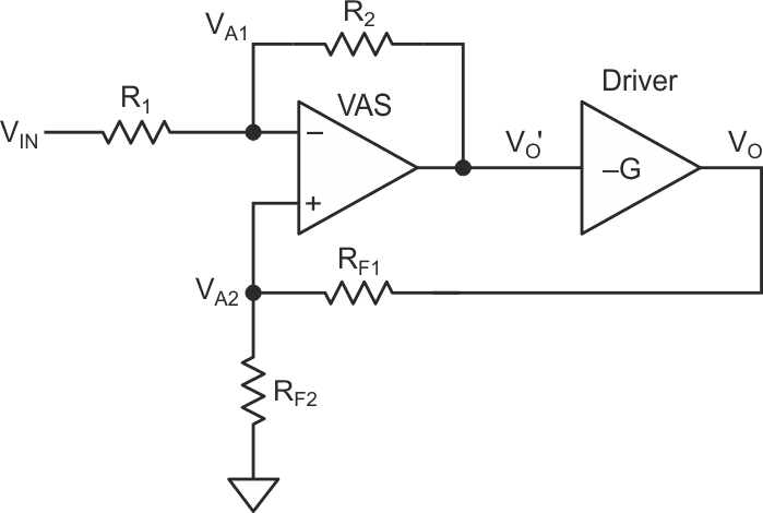
The VAS (voltage amplifier stage) is, as the name states, the system element that amplifies the signal that comes from the input, driving the AB stage through the driver stage (usually a common emitter). The driver is connected to the AB stage, a complementary emitter-follower that provides high current gain. Finally, the negative feedback loop, which affects the gain of the VAS stage, makes the whole system linear and stable.
The VAS stage is usually built using a differential amplifier architecture, where one side of it receives the input signal, and the other, the negative feedback signal. For the sake of simplicity, let’s replace the VAS with an op amp (just to illustrate the offset issue) and analyze the relationship between the stages and the offset we have been talking about a bit more mathematically.
Figure 4 shows a simplified VAS and a driver. This simple model will provide us with valuable insights about the output DC offset. R1 and R2 form a local negative feedback, while RF1 and RF2 form the global negative feedback network. The driver, which is usually a common emitter stage, yields a negative gain –G. For simplicity, the AB stage is neglected, since for an emitter-follower the voltage gain is approximately –1.
 |
|
| Figure 4. | This simplified model of a VAS and driver will provide us with valuable insights about the output DC offset. |
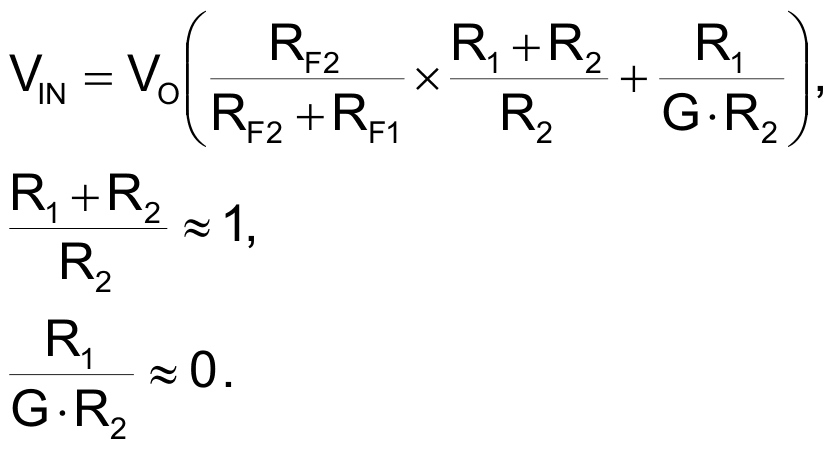
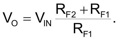
The VAS gain is determined by the relationship between R1 and R2, R2 >> R1 and VA1 = VA2 = VA. The driver gain is very high, so the whole amplifier gain is determined by the relationship between RF1 and RF2:
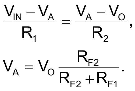
Replacing VA and operating we get:
 |
(1) |
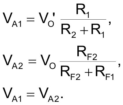
This is not such an impressive conclusion, so let’s analyze the relationship between VO and the voltage at the input of the driver, VO’, with the input grounded:
 |
(2) |
This last equation is very important because it shows the relationship between the DC voltage of the driver stage and the output DC voltage of the amplifier, indicating that a small fluctuation of VO’, would generate a big offset in VO.
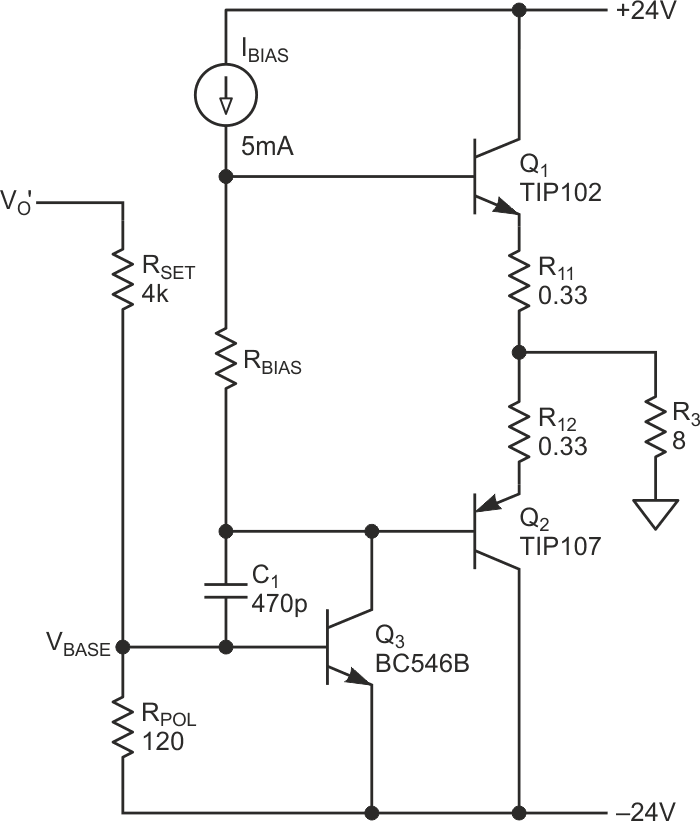
As mentioned earlier, the driver stage is usually composed of a simple common-emitter stage (Q3 in Fig. 1), with a small resistor (RPOL) that fixes the required base to emitter voltage. This transistor provides the base current for the output transistors, so it’s not rare to have a collector current in the milliamps range for this stage.
Let’s forget about temperature effects for a while, so when we turn on the circuit for the first time, we calibrate the VAS so that the output DC voltage is in the middle of VCC and VEE, zero volts. If no signal is applied, since the AB stage is a voltage follower (common collector) the driver transistor Q3 is holding most of the VEE voltage (VEE – VBE), through Q3 is flowing the bias current IBIAS, so Q3 is dissipating an approximate power given by:

That power is heating Q3, and that heat changes the device’s VBE at a known rate of –2.2 mV/°C, thus changing the output DC voltage that was adjusted previously.
If the transistor starts to heat, say 40 °C above ambient temperature, its VBE will drop by roughly 88 mV.
This smaller VBE requirement that occurs while the transistor temperature rises is what makes the VO’ (voltage explained previously) at the output of the VAS change accordingly, hence producing a DC voltage drift at the output.
A real-life example
The circuit in Figure 5 illustrates what has been explained so far.
 |
|
| Figure 5. | This is a first-order real-world implementation of the circuit. |
To keep offset low, it’s convenient to set VO’ as close to zero as possible. This is the purpose of RSET, which represents a multi-turn trimmer.
Here the relationship between the base voltage and VO’ is:

So the output voltage drift based on base-emitter voltage change is:
 |
(3) |
With this equation we can calculate how much the output voltage will change for each °C change in the driver transistor, if we assign values to the components (taken from a real amplifier), for example:

VO = –12.8 mV/°C,
PQ3 ≈ 24 V × 5 mA = 0.12 W.
Let’s suppose that Q3 is housed in a TO-92 package. In this case, the junction temperature increment can be calculated using the junction-to-ambient thermal resistance for this package:
RΘJA = 200 °C/W,
ΔTEMP = 200 °C/W × 0.12 W = 24 °C,
ΔVO = 24 °C × (–12.8 mV/°C) = –305 mV.
In conclusion, if no compensation is applied, the output will drift about 305 mV. This is only considering the self-heating effect of the transistor. This offset could increase if the ambient temperature rises for any reason.
How to mitigate this effect
The base-emitter voltage of Q3 is fixed by RPOL, so one way to compensate the VBE voltage change would be to make RPOL somehow follow this variation. This could be achieved using a temperature-dependent resistor as RPOL attached to the transistor, like a thermistor. Since the VBE change rate is negative, the thermistor would have to be NTC.
Let’s calculate the thermal coefficient required for RPOL.
IR_POL (which can be considered constant) flows through RPOL, and VBE is equal to VR_POL:
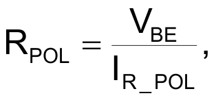
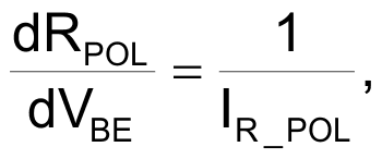

In our example RPOL = 120 Ω and IR_POL = 5.6 mA, so:

We need to find a thermistor with that exact thermal coefficient and resistance value at 25 °C. Since this is not possible because most NTC thermistors have a much higher temperature coefficient, the solution is to parallel a higher value thermistor or thermistors with RPOL.
This is the equation that models a thermistor’s temperature dependence:

where RTH0 is the thermistor resistance at ambient temperature (what we want to calculate), B is a parameter, typically 3400°K, and T is the absolute temperature, with T0 being the ambient temperature, approximately 298.16°K.
So the slope at ambient temperature can be calculated like this:

This is the resistance change rate per °C:

The thermistor is in parallel with RPOL:
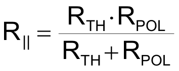
and:

With this we obtain the parallel resistance variation:

And replacing with the thermistor resistance delta per °C:

We can now calculate Rth0 for the example we are analyzing:

RTH0 = 1.12 kΩ.
For the sake of practicality, the value of the thermistor can be rounded to 1.2 kΩ.
Considerations
The thermistor should be much smaller than the transistor, so the temperature of the thermistor will be equal or very approximate to the temperature of the transistor case. This will also reduce the thermal inertia, making the system reach the steady state faster. The thermistor should be attached to the transistor case using thermal adhesive.
Testing the concept
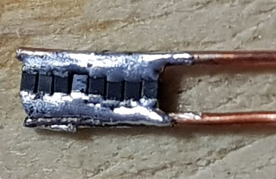
In order to determine how accurately the concept modeled the circuit’s real-world behavior, I constructed a test circuit. Since a 1.2 kΩ thermistor (NTC 0402) was not available, I wired eight 10 kΩ thermistors (0402 Murata NCP15XH103D03RC) in parallel (Figure 6) to produce a very similar value (1250 Ω). Note that connecting thermistors in parallel won’t change the temperature coefficient we calculated.
 |
|
| Figure 6. | This is a 1.25 kΩ thermistor made from eight 10 kΩ thermistors wired in parallel. |
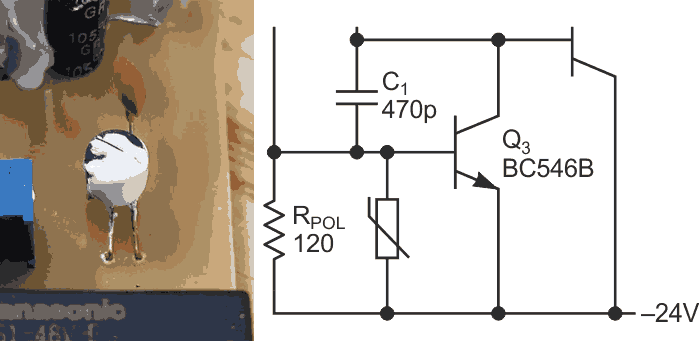
Then, using thermal adhesive I attached the sensor to the flat side of Q3 (Figure 7), and connected it in parallel with RPOL (that is an SMD resistor at the other side of the board).
 |
|
| Figure 7. | The thermistor shown in the prior schematic (Fig. 6) is thermally bonded to Q3. |
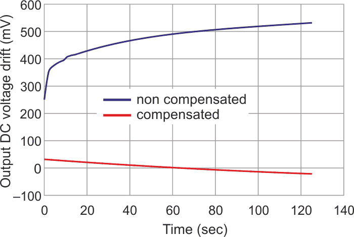
Finally, in Figure 8 here we can see the output voltage drift with (red line) and without (blue line) the thermistor connected, where the steady state is reached after approximately 2 minutes.
 |
|
| Figure 8. | Here we can see the output voltage drift with (red line) and without (blue line) the thermistor connected. |
The circuit’s compensated response (red line) is considerably flatter than the uncompensated response (blue line), a sign that the compensation is working. The fact that the slope is negative could mean that it’s a bit over compensated, but this is not a problem, since the DC drift is still very small.
It’s also worth mentioning that we calculated the required temperature coefficient at 25 °C, but the thermistor is not linear. This means that the temperature coefficient is not constant over the entire range. But, since the compensation is intended to work within a limited temperature range, it’s safe to neglect the non-linearity of the thermistor.
