Computer Terminal Corporation (now defunct Datapoint) launched the DataPoint 3300 computer terminal in 1969 as a platform to replace teleprinters, or the precursors to fax machines. The machine was implemented using TTL logic in a mix of small- and medium-scale integrated circuits (ICs), which could produce an enormous amount of heat during operation.

When the terminal was announced in 1967, RAM was extremely expensive (and heavy). So, the DataPoint terminal stored its display of 25 rows of 72 columns of upper-case characters using fifty-four 200-bit shift registers, arranged in six tracks of nine packs each, providing shift register memory for 1,800 6-bit characters.
To address the excessive heat and other issues, CTC designed the DataPoint 3300’s predecessor with a CPU, placing all of those ICs on a single chip. CTC co-founder Austin Roche looked to Intel to help with the endeavor, as the company was well known for being a primary vendor of RAM chips at the time.
Bob Noyce and the 4-Bit 4004
However, the company found promise with the production of its first programmable microprocessor – the 4-bit 4004. Roche took his processor design, reportedly drawn on tablecloths in a private club, and met with Intel founder Bob Noyce.
Roche presented his design as a potentially revolutionary development and suggested Intel could develop the chip at its own expense and sell it to the companies that would surely come knocking, including CTC. Noyce expressed his concern with the processor concept, saying that it was an intriguing idea and Intel could definitely manufacture the processor, but it would be a dumb move.
Noyce thought that if you had a computer chip, you could only sell one chip per computer, but with memory, you could sell hundreds of chips per computer. Noyce was also concerned about his existing customer base. Intel was already selling a healthy amount of RAM chips to computer manufacturers. If the company started making CPUs, would those existing customers look at Intel as competition and go elsewhere for RAM?
The 8-bit 8008
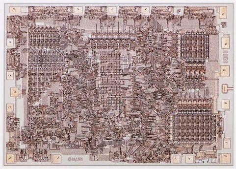
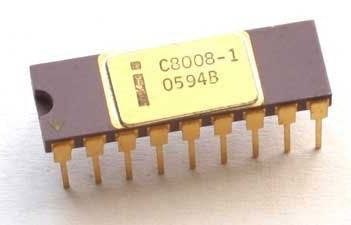
Noyce eventually agreed to develop the chip with a $50,000 contract in 1970, with Texas Instruments coming on board as a second supplier. The journey toward the creation of Intel’s 8008 (Fig. 1) began in the 1960s with the success of its memory chips and the development of CTC’s microcontroller. Engineers used the latter to design a groundbreaking new processor that could drive a range of applications from calculators to control systems.
 |
|
| Figure 1. | Intel’s C8008-1 variant packed 3,500 transistors in an 18-pin dual-inline package and maxed out at 800 kHz. |
The 8008 8-bit powerhouse offered a compact design, low power consumption, and impressive performance capabilities. It was a commercial success.
Initial versions of the 8008 maxed out at 0.5 MHz and could access significantly more RAM than its predecessor, the 4004. The chip still utilized Roche’s architecture, featured an 8-bit data bus, and could address up to 16 kB of memory, opening up new possibilities for software developers and engineers.
Despite its popularity, the 8008 faced some challenges in gaining widespread adoption. Its high cost and limited performance made it impractical for some applications, limiting its appeal to unheard of markets at the time, such as embedded systems and industrial control units. However, it was successful in demonstrating the potential for microchip-based computing, setting Intel on the path to developing the 8080, which it introduced in 1974.
Carving a path to the x86
The 8080 represented a significant improvement over Intel’s previous microprocessors, delivering higher clock speeds, increased performance, and enhanced capabilities. Its success paved the way for the emergence of the x86 architecture, which would go on to dominate the computing landscape for decades.
The x86 architecture was introduced with the 8086 processor, which was designed for general-purpose computing, suiting it for a wide range of applications, including personal computers. With its 16-bit architecture, the 8086 could process more data than the 8080, plowing a path for a new generation of computers that were faster and capable of handling more demanding tasks.
The actual breakthrough for the x86 architecture came with the introduction of Intel’s 8088 in 1979. The chip was a cut-down version of the 8086, offering an 8-bit external data bus that made it compatible with 8-bit peripherals and memory systems. While the reduced performance may seem counterintuitive, the 8088’s lower cost made it an ideal solution for the burgeoning PC market.
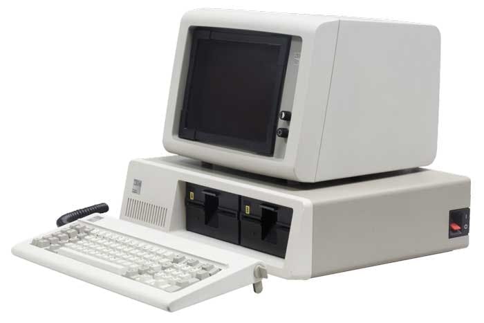
In 1981, IBM took advantage of that low cost and introduced its model 5051 personal computer (Fig. 2), which boasted an 8088 (at 4.77 MHz) and up to 256 kB of RAM and competed with Tandy, Apple, and Commodore, which dominated the market during that time.
 |
|
| Figure 2. | IBM’s 5150 featured an 8088 Intel processor, up to 256 kB of RAM, and 5.25 floppy or cassette drives for data storage. |
The enduring legacy of the x86
In the years that followed the 8088, Intel continued to refine and expand the x86 architecture, introducing a series of more powerful and feature-rich processors. The x86 platform has stood the test of time, moving from 8-bit in the 1970s to 64-bit (aka x86-64) in the 2000s.
Last year, in 2023, the company proposed a significant change to the architecture, now known as x86-S (with S standing for "simplification"). Support for legacy execution modes and instructions would be removed, meaning it will primarily support 64-bit systems.
Today, the x86 architecture remains a cornerstone in the computing industry, driving a wide range of devices, including desktops, laptops, servers, and workstations. Its lasting legacy can be traced back to the humble beginnings of Intel’s 8008 processor, whose innovative design and groundbreaking capabilities laid the foundation for one of the most successful architectures in computing history – a far cry from being a dumb move.