Designers charged with creating precision analog front ends and signal chains know that the performance of the voltage reference – whether a discrete standalone device or one that’s embedded in a component such as the analog-to-digital converter (ADC) – is often the ultimate determinant of system performance. An accurate, stable reference enables the system to not only do what it needs to do, but also “calibrates out” other system imperfections.

For this reason, IC vendors have pushed performance of these reference ICs with advanced designs, processes, and packaging. The result has been impressive performance with extremely low temperature coefficients, which are often the ultimate challenge for this class of component that strives to do one thing and one thing only.
For some applications, however, even being “extremely good” isn’t quite good enough. To achieve even better performance, keeping the voltage reference core at a constant temperature is key to maintaining a stable reference output.
Leveraging buried Zener tech and on-chip heater
That’s where Analog Devices’ (ADI) ADR1001 provides a tiny, easy-to-use solution. This device is a fully integrated, ultra-low drift, buried Zener precision voltage-reference solution in a single chip (Fig. 1).
 |
|
| Figure 1. | The block diagram of the Analog Devices ADR1001 precision voltage reference, including surrounding schematic, shows split-supply heater operation and 10-V reference output. |
The on-chip heater (sometimes referred to as “ovenization”) is combined with ADI’s buried Zener technology, allowing the ADR1001 to achieve sub-ppm temperature-coefficient performance and single-digit ppm long-term drift performance. By integrating all of the entire signal-conditioning circuitry required by the LTZ1000, it significantly reduces overall solution area while simplifying the design process by eliminating the many challenges of building a discrete circuit solution.
Voltage reference’s ease of use
In addition to delivering extreme precision across critical parameters, the ADR1001 incorporates ease-of-use features to reduce cost and design-in effort. These include a pin-programmable internal thermostat, resistor-programmable heater current limit, open-collector power-good flag pin, hermetic surface-mount package, and an extra matched-resistor pair. By default, the internal heater’s temperature setpoint is 70 °C when no external resistor is connected to the TSET pin.
Operating from a 9- to 36-V supply, the device embeds a 6.6-V reference and resistive divider to produce a precision 5-V output that can be easily “boosted” using those matched resistors. The divider network and output buffer combination are trimmed to within ±0.25% initial accuracy. The resistor pair also enables designers to easily generate a negative voltage reference or a gain-of-2 with minimal impact on the output accuracy or drift. The 5-V output noise (0.1 to 10 Hz) is just 0.13 ppm (peak-to-peak).
Of course, using a stabilizing heater comes at a cost in power consumption, but that’s a tradeoff designers may be very willing to accept. The heater current limit is 100 mA when its limit connection is shorted to heater ground.
The 21-page datasheet include performance specifications and drift/accuracy graphs (long and short term), many based on a brief 15-second delay after power-up. It also includes some useful application-connection schematic diagrams such as basic hook-up, simultaneous full 5-V and half-scale 2.5-V reference outputs using an external buffer, creation of a 10-V ultra-stable reference, and development of a bipolar ±5-V digital-to-analog converter (DAC) drive using an external op amp.
Eval board for voltage reference
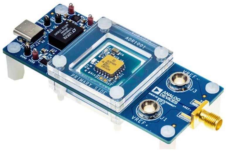
Users of even a functionally simple device such as this reference can benefit from an easy way to exercise and evaluate operation. To this end, Analog Devices offers the ADR1001E-EBZ evaluation board (Fig. 2). The 6.6-V Zener output is divided down to a precision-trimmed 5 V and is routed to both banana jacks and an edge-mounted SMA connector.
 |
|
| Figure 2. | The companion ADR1001E-EBZ evaluation board provides a 5-V output via an SMA connector, as well as banana jacks. |
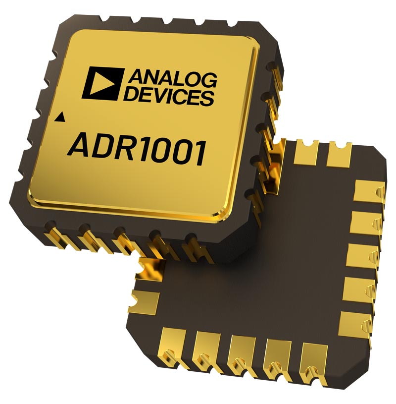
The ADR1001 is packaged in a hermetically sealed ceramic, 20-terminal, leadless chip carrier (LCC). (See Fig. 3)Thanks to this surface-mount ceramic package, users can eliminate the through-hole component soldering step while still retaining the hermetic seal of a classic through-hole metal-can package.
 |
|
| Figure 3. | A hermetically sealed ceramic, 20-terminal, LCC package. |
