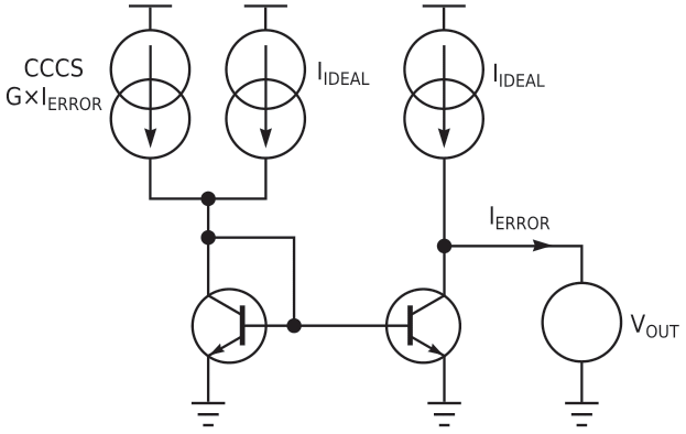
Simulating the output-offset current of a current mirror is straightforward. You simply have to apply an input current, measure the output current, and calculate the difference. This output-offset current, however, is not equal to the input-offset current, especially when the circuit is not a 1-to-1 mirror. Simulating the input-offset current with high accuracy is more complicated. Suppose you're dealing with a 1-to-1 mirror and you want to know what input current is needed to obtain an output current of 10 µA. Ideally, the input current would be 10 µA, assuming that the input offset current is zero. However, because of the finite beta of bipolar transistors, finite output impedances, mismatches, and so on, the input offset current is not equal to zero. The design in Figure 1 provides high accuracy and a low simulation time.
 |
|
| Figure 1. | Use this circuit for simulation of current-mirror input-offset currents. |
You use feedback to force the current of a CCCS (current-controlled current source) to equal the input-offset current. The current that flows into voltage source VOUT is the difference between the output current of the mirror and the ideal output current. This current is the “error current” (IERROR). When the CCCS equals the input-offset current, then the error current is zero. The high-gain CCCS amplifies the error current, and the CCCS adds to the input current. In this way, you create a feedback loop, and the current that you measure through the CCCS is the input-offset current. The feedback loop implements a high gain that ensures a high accuracy (negligible error current). And, because you obtain the result by calculating the dc operating point, the simulation time is small.
 |
|
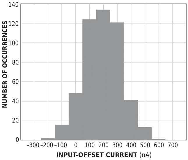
| Figure 2. | This bar graph shows the input offset-current distribution. |
Figure 2 shows simulation results of 500 Monte Carlo runs for IIDEAL = 10 µA, gain G = 1000, and VOUT = 1 V. The npn transistors have an emitter length of 40 microns and use a 0.35-micron silicon-germanium BiCMOS process, but you can use the simulation method for all current mirrors and all types of transistors. The average of the distribution in Figure 2 is 194 nA, and the standard deviation is 131 nA. The average is not zero because of the base-current error.