The concept of using supercapacitors (also known as ultracapacitors, supercaps, etc.), and replacing the batteries in portable micropower applications (Ref. 1) is gaining momentum. In fact, it has become one of the more noticeable technical trends of recent time.
Supercapacitors, when used as a power source, hold tremendous advantages over traditional rechargeable batteries. For instance, they feature high endurance to short circuits, very short charging cycle, and practically unlimited charge-discharge cyclomatic durability (up to 1 million cycles compared to 1000 for batteries), thus providing an environmentally clean, “no-disposable- part” solution. In addition, most supercaps comply with the European Union’s Restrictions on Hazardous Substances (RoHS).
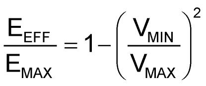
The fundamental difference between supercaps and batteries from a design prospective is the substantial voltage change during a capacitor’s charge/discharge cycles, which goes theoretically from zero to the maximum rated voltage, while a battery’s terminal voltage varies just a little during its operational cycle. Supercaps are the subset of electrical capacitors. Thus, the effective energy, EEFF , that can be obtained from a supercap during its discharge cycle, when the terminal voltage changes from the maximum, VMAX, to the minimal operating voltage, VMIN, of the powered device could be calculated as:
 |
(1) |
Correspondingly, the effective energy ratio (EER) could be defined as:
 |
(2) |
where EMAX stands for the total energy stored in the capacitor. Equation 2 clearly indicates that the effective energy ratio increases dramatically as we lower the minimum operational voltage VMIN of the powered electronic circuit due to the lower amount of residual electrical energy left in the capacitor. EER is a very important design consideration to be applied to any capacitor-powered electronic circuit.
 |
|
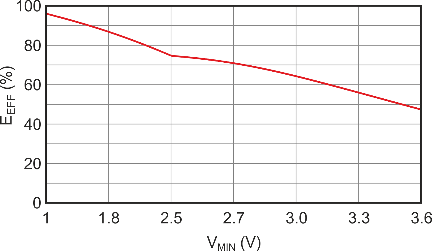
| Figure 1. | The graph of capacitor effective energy ratio (EER) for VMAX = 5 V shows a dramatic decrease as VMIN increases from 1.0 V to 3.6 V. |
The Table 1 and the corresponding graph in Figure 1 show a sample EER calculated for a capacitor-powered circuit with maximum terminal voltage VMAX = 5 V. It’s quite noticeable that EER increases from 48% to 96% when the minimal operational voltage, VMIN, of the powered electronic device changes from 3.6 V to 1 V. Therefore, “squeezing the device operating voltage” is the primary design consideration of capacitor-powered electronics.
| Table 1. | EER for VMAX = 5 V | ||||||||||||||||
|
|||||||||||||||||
The goal could be achieved by using an ultra-low-power dc-dc boost converter (e.g., the inductor-less type described in Reference 2, operating from as low as 0.7 V), but it could add to the design cost and energy consumption. The second alternative is to use a special design technique targeted at providing ultra-low-voltage device operation.
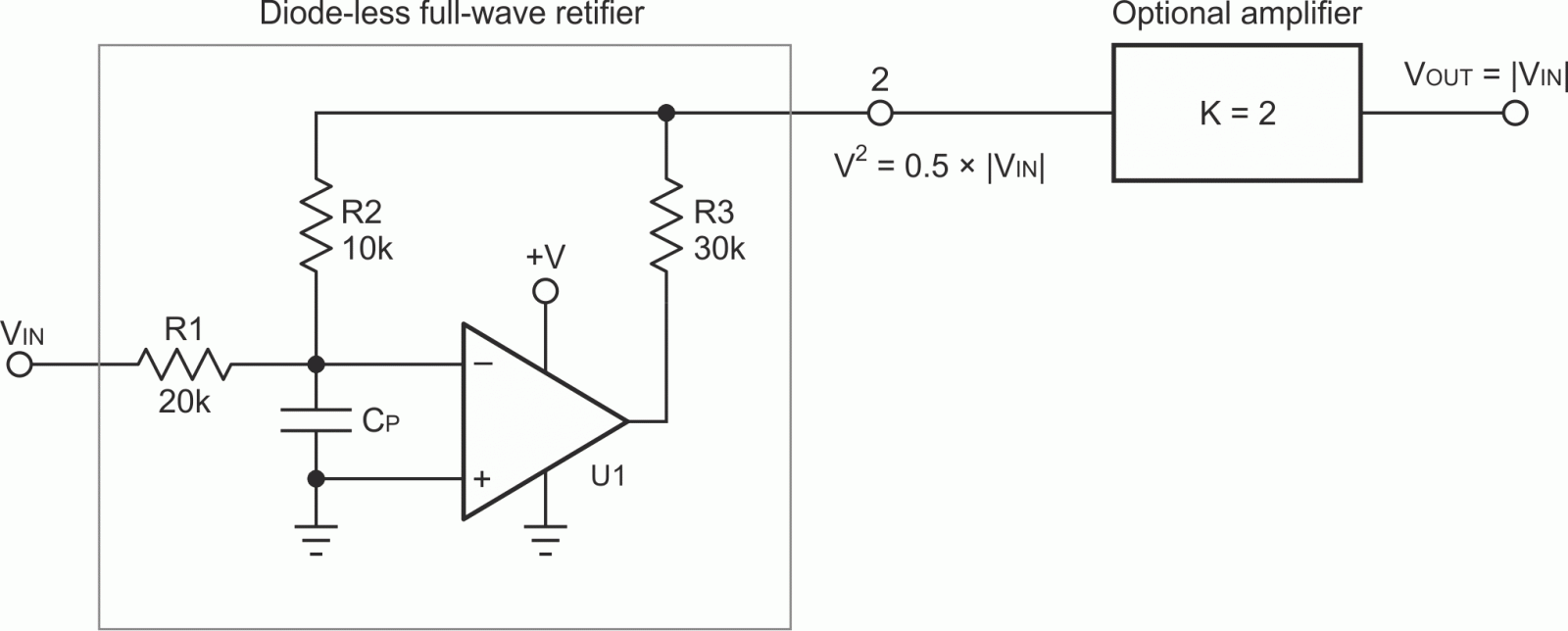
A good example of such low-voltage circuit design is described in Reference 3. The suggested micropower, ultra-low-voltage, fullwave, diode-less rectifier is an excellent fit for the design paradigm of capacitor-powered electronics (Fig. 2).
 |
|
| Figure 2. | The diode-less precision full-wave rectifier in its simplest form employs a single rail-to-rail op amp and three matched resistors. |
To understand the operational principle of the circuit, it’s important to notice that the op amp works in a single-supply mode. If a positive signal is applied to the input (VIN > 0), the op-amp output goes to zero and the whole circuit virtually transforms itself into a simple passive network of three resistors – R1, R2, and R3 – connected in series. When the input signal goes negative, the op amp returns to “normal linear life” and performs like a regular inverting amplifier. To produce the symmetrical output for both negative and positive half-waves, R1, R2, and R3 must be selected to comply with the mathematical condition:
 |
(3) |
As the condition of Equation 3 is fulfilled, the circuit has a gain of one-half at point 2 in the circuit. An optional non-inverting amplifier with a gain of two could be added to produce the overall unity gain, providing the operational equation of VOUT = |VIN|.
The circuit has certain limitations: its input resistance is different for the positive and negative half-waves. Theoretically, resistance is R1 + R2 + R3 for the positive and just R1 for the negative signals. Also, the input parasitic capacitance, CP, of the op amp affects the ac mode operation, especially in the high-frequency range. (Detailed analysis of ac performance goes far beyond the scope of this article. I would recommend using Spice simulation for the practical design).
The circuit could employ a variety of rail-to-rail micropower op amps – for example, the dual LMC6442 (VMIN = 1.8 V), the dual MAX4289 (VMIN = 1.0 V), or a similar type.
Since a typical silicon diode has a forward-voltage drop of about 0.6 V, output dynamic range is reduced to “consuming” that very 0.6 V from the supply voltage. This consideration has become rather important in the case of building capacitor-powered electronics, where the circuit supply voltage should go as low as possible. For this reason, the suggested diode-less design is a better fit when running in capacitor-powered mode. It saves the valuable 0.6 V (which is a rather significant value considering the possibility of an op amp running at 1 V), and thus squeezes the minimum operating voltage of the circuit and increases the overall EER of the solution.
References
- Bell, Alexander, “Single Capacitor Powers Audio Mixer,” EDN, Mar. 14, 1997.
- Bell, Alexander, “Single niCd Cells Drive Op Amp,” EDN, Dec. 5, 1996.
- Bell, Alexander, “Simple Full-Wave Rectifier,” Electronic Design, Apr. 4, 1994, p. 78.