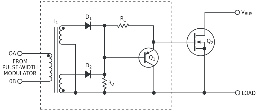
The low- to moderate-power system in Figure 1 provides the interface between a pulse-width modulator and a high-side IGBT (insulated-gate-bipolar-transistor) or MOSFET switch. You can use it to interface TTL or CMOS circuitry to an H-bridge if you buffer it by a FET driver, such as an ICL7667 or an MIC4423. When OA is positive, D1 conducts, charging the capacitance of the FET through R1. The value of R1 and the output impedance associated with the drive signal determine the turn-on time of the FET. After the capacitance is charged, the voltage across R1 is essentially 0 V, and Q1 is off. During the PWM dead time, the gate capacitance discharges through Q1 and R2. R2 and the hFE of Q1 determine the turn-off time of the FET. This circuit achieves turn-on and -off times of less than 150 nsec.
 |
|
| Figure 1. | You can use this low-cost circuit to drive high-side FETs or IGBTs. |
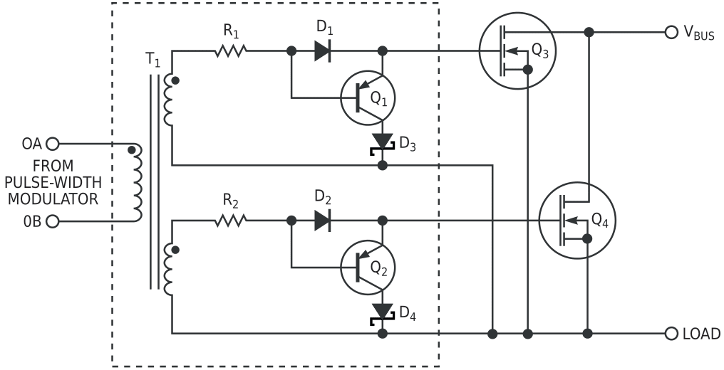
In systems that require higher power, you can use a dual-FET circuit (Figure 2). R1 and R2 and the output impedance of the PWM or FET driver determine the turn-on time. R1 and R2 and the hFE values for Q1 and Q2 determine the turn-off time. The Schottky diodes, D3 and D4, prevent current flow through the collector-base junctions of Q1 and Q2 when the drive signal is negative. You can obtain switching speeds higher than 50 nsec at turn-on and 100 nsec at turn-off with this circuit, depending on the output impedance of the transformer drive signal.
 |
|
| Figure 2. | Two FETs in parallel provide more power than the circuit in Figure 1. |