Designers tend to favor forward- and flyback- converter topologies for loads less than 200 W because they are simple and can power multiple isolated outputs. Their simplicity is partially based on the fact that these converters use a single ground-referenced transistor switch to drive the transformer’s primary. The drawback to this approach is that the voltage stress on the transistor is the sum of the bus voltage, the reflected transformer voltage, and the turn-off leakage-inductance spike. If you add a second high-side transistor switch, the voltage stress reduces to the bus voltage only. For many applications, the added complexity and parts count is a small price to pay for the benefits you receive.
Two-switch forward converter
 |
|
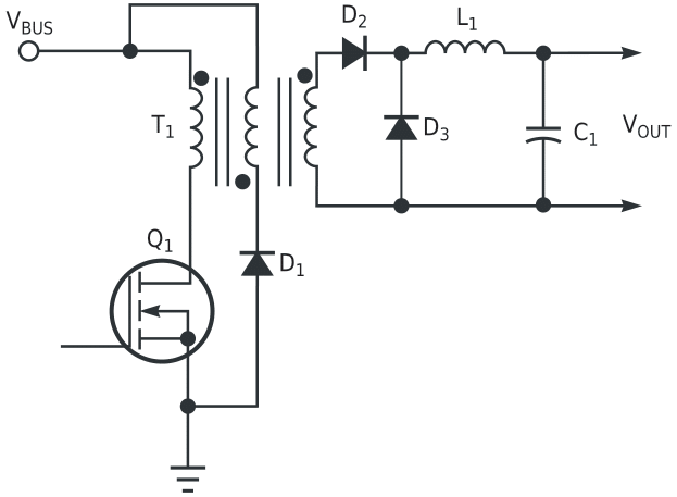
| Figure 1. | The traditional forward converter puts a comparatively large voltage stress on the switching transistor. |
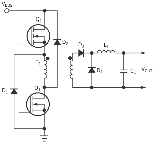
A simplified forward-converter power stage comprises a single transistor switch (Q1), power transformer (T1), reset diode (D1), output rectifiers (D2 and D3), and filter (L1 and C1) (Figure 1). As in the single-switch example, the simplified two-switch forward converter keeps the original transistor switch, Q1, in series between the low side of the transformer and ground (Figure 2). A second transistor, Q2, wired in series between VBUS and the high side of the transformer primary, turns on and off simultaneously with Q1. When both transistors are on, they deliver power through the transformer and the output filter to the load. As the transistors turn off, D1 and D2 clamp the voltage on the primary winding to ground and VBUS respectively. At that time, each transistor has a turn-off voltage stress of VBUS.
 |
|
| Figure 2. | A two-switch topology reduces the transistors’ voltage stress to the bus voltage. |
Not only do D1 and D2 clamp the energy from the transformer magnetizing inductance, but more importantly, they clamp T1’s leakage inductance as well. The switching transistors do not have to dissipate the energy stored in the leakage inductance during the on-time nor does the design have to resort to resistive snubbers to dispose of the energy. The advantage of this approach over a single-switch arrangement is reduced system losses and system noise, because it effectively clamps the ringing normally associated with the release of the inductive energy.
Single-switch forward converters most often reset their cores through an additional reset winding. When Q1 turns off, the voltage on the reset winding reverses until D1 clamps it at the bus voltage. If the reset winding has the same number of turns as the primary winding, then the core always resets with a reset time equal to the on-time of the transistor. The voltage stress on the switching transistor will be twice the bus voltage plus the leakage energy spike. The core will always reset, provided that the maximum on-time is less than 50%. Designers keep the on-time within this limit by choosing the turns ratio so that at the minimum line voltage, the maximum required duty cycle is 40 to 45%. Many of the popular PWM IC controllers have duty cycles limited to less than 50% for added protection during any anomalous condition. The two-switch forward converter resets the transformer in the same way without the additional reset winding.
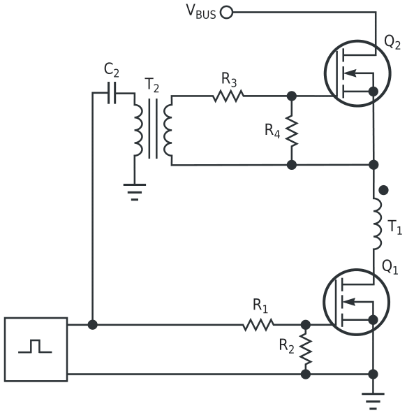
The benefits come at a modest cost. First, the two-switch topology adds a FET switch and a clamp diode. Because the duty cycle is less than 50%, by design, a transformer can provide the isolation for the high-side transistor’s gate drive (Figure 3). A number of other isolated gate-drive techniques can provide the isolated high-side gate drive. Assuming that sufficient gate-drive power is available from a driver, the total additional parts count is five components, including the FET.
 |
|
| Figure 3. | A simple transformer isolated gate drive synchronously operates both primary-side switches. |
Clamping the maximum transistor voltages to VBUS removes any uncertainty about the peak-voltage stress, which, in the single-switch approach is proportional to the value of leakage inductance, the switching speed, and the circuit layout. Leakage inductance is difficult to control and often varies in production.
The series-conduction loss of the high-side transistor FET appears as additional power dissipation. However, if you look at the RDS(ON) (drain-to-source on-resistance) of lower voltage FETs you’ll find that two lower- voltage devices in series have a lower net RDS(ON) than a single higher voltage part. For a single-switch forward converter with a 36 to 78 V input bus application, a 200 V FET is often used provided the leakage-inductance spike is controlled. ON Semiconductor’s MTP20N20E might be a good choice; it has a specified RDS(ON) of 0.16 Ω. For a two-switch application, you can use a 100 V FET instead of a 200 V part. A lower voltage FET with an equivalent die size will have a much lower RDS(ON). A similar 100 V rated part, the MTP33N10E, has a specified RDS(ON) of 0.06 Ω. Even with two switches in series, the total RDS(ON) is 0.12 Ω. So two lower voltage rated parts in series may have a lower total RDS(ON). A comparison between 1000 V and FETs of the same die size leads to an RDS(ON) difference of as much as 5 to 1.
Switching losses and gate-drive losses are obviously higher with two switches, but with lower RDS(ON) devices and the elimination of leakage-inductance loss, efficiency often increases. The elimination of snubber components and control of the leakage-inductance effects are significant benefits of the two-switch approach, especially at higher input bus voltages. Higher bus voltage applications often have more primary turns, which tends to increase leakage inductance and loss. The benefits of the two-switch approach increase with increasing bus voltage but lower bus voltage applications can often benefit as well.
Two-switch flyback operation
 |
|
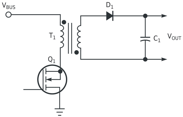
| Figure 4. | The traditional flyback converter puts a voltage stress on the switching transistor comparable with the stress of the one-switch forward converter. |
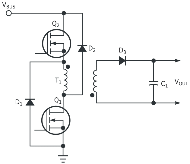
The main components of a flyback-converter power stage are the single transistor switch, (Q1), the power transformer, (T1), the output rectifier (D1), and the filter capacitor (C1) (Figure 4). A simplified two-switch version retains the original transistor switch, Q1, in series between the low side of the transformer and ground. This topology adds Q2 in series between VBUS and the high-side of the transformer primary (Figure 5). As in the two-switch forward converter, the driver turns on both transistors at the same time. The two-switch flyback converter realizes all of the same benefits of the two-switch forward converter. Diodes clamp the transistor switches and return the leakage-inductance energy to the bus in place of snubbers. You can use the same simple gate drive for the high-side transistor FET and operate the two-switch flyback converter in either discontinuous- or continuous- conduction mode as with the two-switch forward-converter.
 |
|
| Figure 5. | Like the forward converter, the two-switch flyback benefits from fixed stresses on the switching components and lower noise. |
