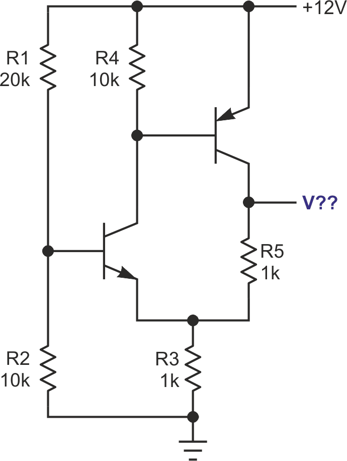
I would sometimes have to interview someone to fill an engineering position in "my" company. Which company that was, changed from time to time, but I needed a way to see just how competent someone was at circuit analysis, somebody with whom I would soon be working. I came up with a circuit which I would present to a candidate and ask him/her to analyze it for me right then and there. After a while, I thought of this circuit as my "weed-eater" because it would weed out anyone who really wasn't good at dealing with analog circuit analysis. It was the following: Two transistors, one NPN and one PNP, are connected as shown in Figure 1. Making a few well-chosen simplifying assumptions, please find the voltage at the collector of the PNP.
 |
|
| Figure 1. | The weed-eater circuit. |
Rather than trying to describe the tortuous paths that were traversed by some interview candidates, I will simply present the assumptions that I expected would be made and the ensuing analysis. The starting assumptions are that the transistors are silicon and will exhibit base to emitter voltages of 0.6 V and that the β values of both transistors are very high so that their base currents are virtually zero.
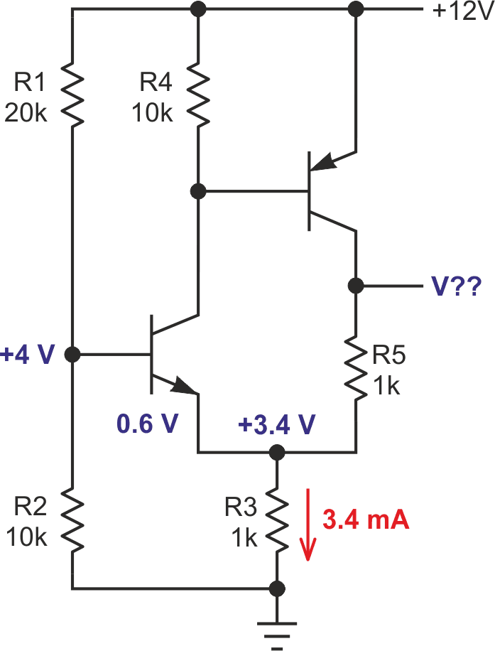
With essentially zero base current to the NPN, R1 and R2 voltage divide the +12 V rail voltage to +4 V at the NPN base (Figure 2). With a VBE of 0.6 V, the NPN emitter is +3.4 V and the current flowing in R3 will be 3.4 mA.
 |
|
| Figure 2. | The first step of the analysis. |
The next issue is, how does that 3.4 mA get shared by the NPN emitter and R5?
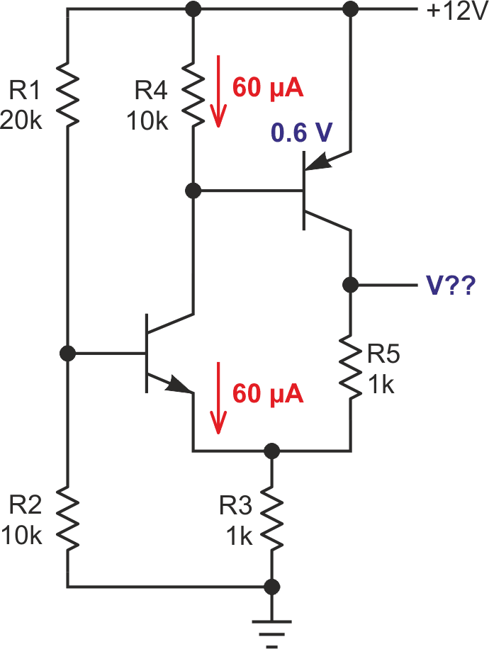
The VBE of the PNP is 0.6 V so that the current flow in R4 is 0.06 mA or 60 µA (Figure 3).. With the PNP base current being virtually zero, that 60 µA becomes the collector current of the NPN which in turn becomes the emitter current of the NPN because of the NPN's extremely high β value.
 |
|
| Figure 3. | The second step of the analysis. |
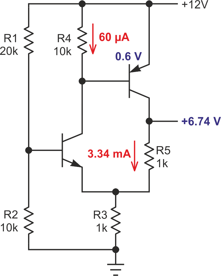
The current flowing through R5 must be the difference between the R3 current of 3.4 mA and the 0.06 mA current of the NPN emitter. That value is 3.4 – 0.06 = 3.34 mA (Figure 4).
 |
|
| Figure 4. | The third step of the analysis. |
The voltage drop across R5 is then 3.34 V which when added to the 3.4 V at the top of R3, puts the top of R5 and the PNP collector at +6.74 V.
Easy, huh?? Well, yes, it is easy but even so, this circuit weeded out a lot of unqualified candidates.
