Capturing transient analog signals with a microcontroller normally involves adding a full-fat peak-hold circuit as an external peripheral. This novel approach minimizes that extra hardware by using a µP’s ability to switch its pins between analog and digital modes on the fly. While this DI specifically uses a PIC, the principle can be applied to any device with that capability.
Figure 1 shows the basics. We may want to add some complications later.
 |
|
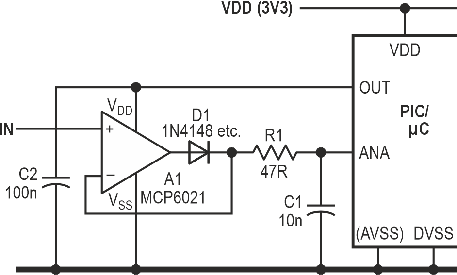
| Figure 1. | The basic peak-hold circuit. The PIC pin labelled ANA samples the voltage on C1 and then resets it to ground, ready for the next sample. |
A1 and D1 form an “active diode”, which rapidly charges C1 to the peak input voltage through R1 whenever A1’s non-inverting input is higher than the diode’s output voltage and hence that on the inverting input. C1 holds its charge as it has no discharge path – leakages excepted – until the PIC needs to sample it, when the ADC is assigned to the relevant input pin (marked as ANA) which starts the acquisition period, during which C1’s charge is shared with the PIC’s internal CHOLD. Once this is done, the conversion can be started, which also immediately disconnects that pin from the ADC, allowing it to be changed from analog input to digital output (active low) to discharge C1, resetting the circuit ready for the next cycle. Thus, a single processor pin performs two functions. Listing 1 shows typical code for the essentials.
Listing 1. Simplified code for capturing the voltage held on C1 and then immediately discharging it to reset the circuit ready for the next sampling cycle.
;; It's assumed you have already configured your chosen pin as
;; an analog input. (It’s given in this example routine as
;; porta,l or ANI/RAI but marked in Figure 1 as ANA.)
;; The exact method of doing this varies widely between PICs,
;; as does the selection of clocks, references, and even the
;; relative priority of analog and digital functions. Beware!
;; Also at the start of the program, clear the digital output
;; for this pin, ready for use as a reset -
bcf PORTA,1 ; pin will be low when it’s an output
;; - and ensure that the pin providing op amp power has been
;; set up as a high digital output. It’s shown as OUT in
;; Figure 1, and here as PORTA,0.
bcf TRISA,0 ; set as an output -
bsf PORTA,0 ; - active high
PeakCapture
;; Assume that the ADC has been assigned to the ANA pin for long
;; enough for stability, when several analog signals are to be
;; sampled, it’s good practice to do that assignment as soon as
;; the previous sample has been taken, meaning that no separate
;; acquisition time needs to be programmed for.
;; Start the conversion on the now-stable analog sample,
bsf ADCONO,GO ; sample the pin (ANI/ANA)
;; Pin can now be changed to digital output (low) to discharge C1.
bcf TRISA,1 ; configures pin as digital output,
; over-riding the analog function
;; Wait until the conversion is complete, during which time C1
;; will be discharging towards ground. This is the best time
;; to select the next analog pin to be sampled, which also
;; minimises wasted cycles.
Loop_ADC
btfsc ADCONO,GO ; loop until conversion is complete
bra Loop_ADC ; - or use goto for sub-18F devices
;; Data’s now available in the A-D result register(s).
;; Restore pin to analog input, ready for next sampling cycle.
bsf TRISA,1 ; reconfigures pin as analog input
Now that we’ve got it working, it’s time to point out its shortcomings and suggest some workarounds.
The voltage across C1 can never be higher than a diode-drop below A1’s VDD, which limits the effective measurement range. (Although a Schottky diode with its lower forward voltage could be used for D1, the higher reverse leakage will compromise accuracy.) If the input must cover the full span, it’s easiest to pot it down first, and either accept a slightly limited resolution on measurements or use a lower reference voltage (2.55 V might be ideal) for the DAC. A1’s VDD can be boosted – see later on – to allow a full positive swing. Similarly, its VSS could be pushed negative if readings needed to be taken very close to ground. Again: see later.
Any input offset in A1 will affect precision. 1 LSB is about 13 mV when using 8 bits with a 3.3 V reference, or ~800 µV with 12 bits, so the allowable offset is half that. (The offset is quoted as being 500 µV at most.)
Note that while C1’s voltage will be measured with respect to the PIC’s AVSS – or perhaps its VREF- pin – it will be discharged to DVSS. (The lower pin-count devices combine AVSS and DVSS on a single ground pin.) Be cautious of any relative offset between them if accuracy is paramount at low input levels. Microcontrollers are often put to sleep during analog measurements to minimize such errors, which can vary according to how hard the device is working.
A more subtle source of errors is inherent in the ADC’s operation. Internally, it uses a small capacitor (CHOLD), anywhere from 10 pF to 120 pF depending on the device’s vintage, to hold the input for processing. The charge on the external capacitor C1 is shared with the internal one during the acquisition time, so unless the ADC is actually connected to the pin when the input pulse arrives, it will read low, scaled by
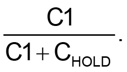
With C1 = 10 nF and if the DAC’s CHOLD = 10 pF, as in the more modern PICs, the error will be ~1 LSB for a 10-bit result, but negligible for 8 bits; lower values of C1 will lead to greater errors.
If that input pulse is shorter than the reset period and arrives while the pin is being held low, it will be attenuated and effectively lost. (And make sure that A1’s decoupling cap can source the inevitable power transient.) Adding an extra MOSFET (extra GPIO pin required, as shown in Figure 2, below) allows ‘instant’ resetting (or around a thousand times faster, probably within a single instruction cycle), and to a genuine ground rather than the PIC’s internal one. (The ADC’s pin would then be left in analog mode.) A cure in ultra-critical situations might be to duplicate the hold circuitry on another pin and sample each channel alternately, selecting the higher reading in code.
In my original application, which was measuring the strength of RF signal bursts, none of these points was a problem, as the input was always between 0.2 and 2.5 V and lasted for hundreds of microseconds, while the output was scaled to read from 0 to 9.
Despite these reservations, this open-loop approach can be faster than the standard configuration which wraps an op-amp round the capacitor. Because C1 is driven directly, the rise-time of the input pulse can now be as fast as you like. A1’s output may overshoot momentarily, but the glitch will be absorbed by the longer time-constant of R1C1.
For accuracy, R1 should be chosen so that the op-amp’s output drive never exceeds its current-limit value, as that would break the feedback loop, resulting in overshoot and a falsely high reading. Also, for clean operation, time-constant R1C1 should be no less than A1’s rail-to-rail slewing time. The 10n + 47R (470 ns is about the same as the measured slew) allowed for accurate measurements of 2.5 V pulses as short as ~3 µs. Experiments showed that R1 could be reduced to 27R, giving a –10% error for 1 µs/2.5 V input pulses.
C1’s discharge time to half an LSB will be

where the latter term will typically be ~100 Ω for PICs working at 3.3 V.
That “≈1.6” is of course
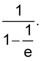
For 8 bits, 10 nF, and 100 Ω; that’s about 14 µs, which can be reduced if you don’t need to measure right down to ground. (Some PICs can struggle there, anyway, especially if they use an internal op-amp in the ADC’s input path.) Choosing to cancel the reset and re-enable the analog input as soon as the A–D conversion finished, which took ~20 µs in my implementation, was more than adequate and simplified the code.
A1 is shown as a Microchip MCP6021 (CMOS, RRIO, 2.5–5.5 V, 10 MHz GBW, <500 µV offset). The MCP6001 is cheaper but less well-specified. As an aside, the dual MCP6022 is great for 5 V experimenting and prototyping because it is available in DIP-8.
As drawn in Figure 1, A1 can be fed from a GPIO pin, allowing it to be powered down when the PIC is asleep. This obviously limits its VDD to the PIC’s supply voltage, restricting the input range as noted above. If you need the full range and a higher switched rail is available, use that; if not, a simple voltage-doubler, probably fed from a PWM output, provides a fix.
The MCP6021’s output drives low to within ~5 mV of its VSS (<1/2 LSB with 8 bits). To operate right down to ground, another voltage-doubler can provide a boosted negative feed, with a simple regulator reducing this to –0.6 V for low-voltage op-amps. Make sure that the total voltage across A1 is within its limits; an extra diode in the positive doubler – D6 in Figure 2 – may be needed to guarantee this. All these add-ons are lumped together in Figure 2. PICs’ pin-protection diodes are rated at 25 mA and should be safe with the increased voltages under any fault conditions. While these simple PIC-driven voltage-doublers are only good for a few milliamps, they could help power other devices if need be.
 |
|
| Figure 2. | Boosting the op-amp’s supply rails can give true rail-to-rail operation while an extra MOSFET allows “instantaneous” resetting of C1. |
All this raises a reality-checking question: what’s powering the upstream circuitry, and is it really delivering a rail-to-rail signal? If not, we don’t need to fuss.
Another reality check: if both boosted rails are available, why not use a higher-voltage, non-RRIO op-amp? The negative regulator Q2/3, etc. then becomes unnecessary.
The extra complications shown in Figure 2 probably won’t be needed here anyway but may come in handy elsewhere.
Largely because of a PIC’s limitations, the simple circuit of Figure 1 is accurate rather than absolutely precise, but has still proved reliable and useful, especially where board space was at a premium. It could also be appropriate as a front end for an external peak-sensing A–D peripheral. The underlying principle could also be used in microprocessor-based kit to clamp a signal line to ground, albeit with 100 Ω or so effectively in series, perhaps where a MOSFET would add too much capacitance.