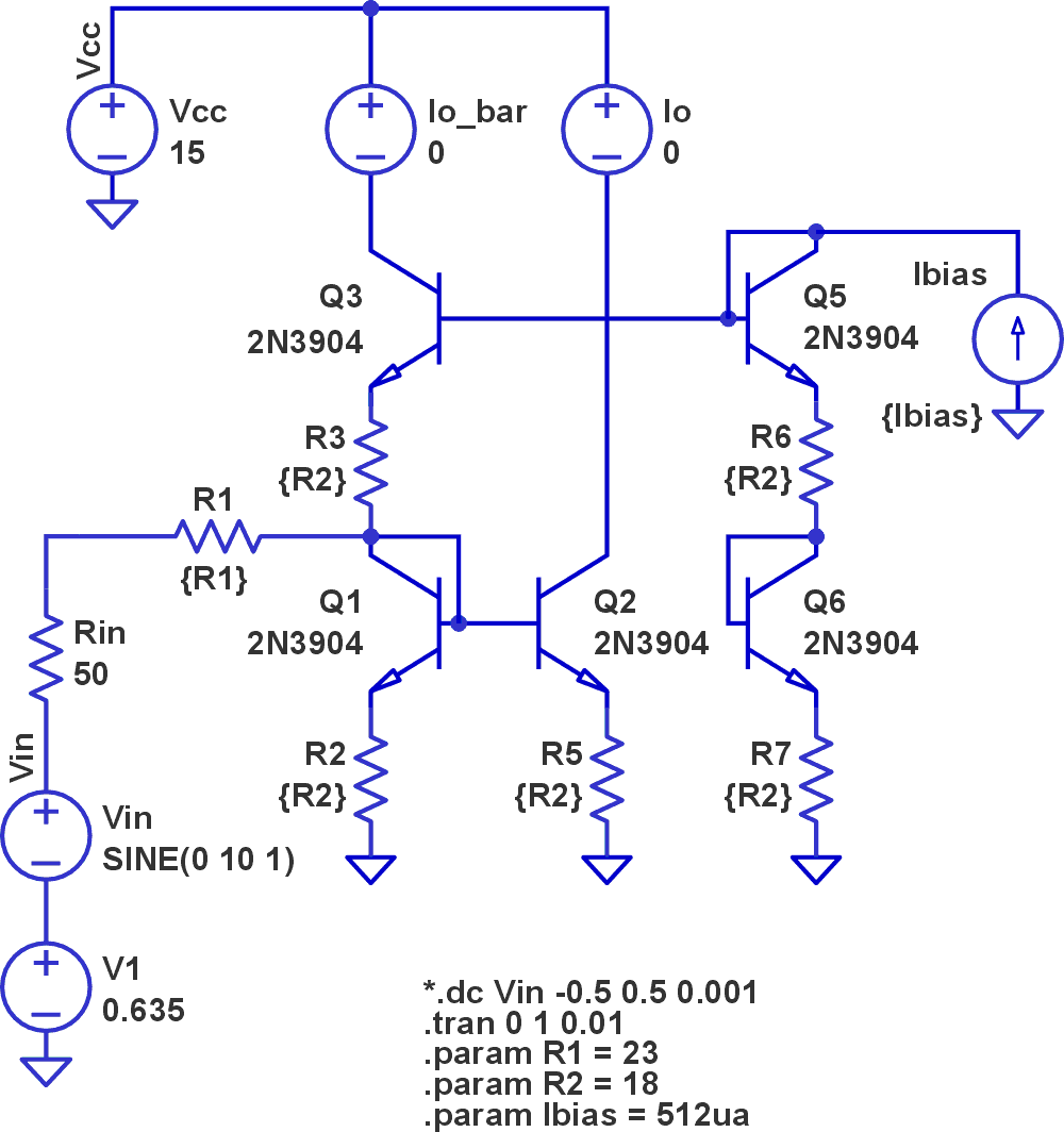
From the micromixer topology by Barrie Gilbert [1], this amplifier allows a single-ended input to be converted to a Class A/B current output from a single supply.
As shown in Figure 1 with an LTspice implementation, the circuit employs 6 bipolar transistors (BJTs) in a unique configuration which “directs” the output current from Q3 and Q4 dependent upon input polarity.
 |
|
| Figure 1. | LTspice schematic of the micromixer topology with 6 BJTs arranged such that the output current from Q3 and Q4 are dependent upon input polarity. |
How it works
C1 serves as a decoupling capacitor which allows the potential at Q1 base to vary from the biased VBE with the Q1 diode connection. Q2 acts as a mirror to Q1 for positive input signals and cuts off for large negative inputs; while Q3 is a cascode under small signal conditions, and sources large negative input currents.
With ideal equal-sized transistors, all collector currents are equal and set by the base-emitter voltages of Q5 plus Q6, which are determined by the current through R3 as IBIAS.
When the input signal is large and positive, input current flows mostly through Q1 which acts as a transconductor and cascode device and Q3 becomes cutoff as its emitter voltage rises. Q2 “mirrors” the Q1 collector current through cascode device Q4, which sinks a replica of the large positive input current as the positive output.
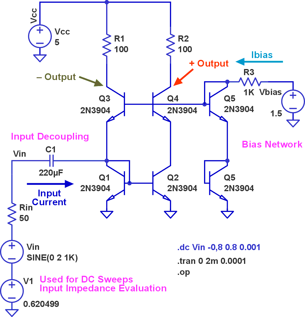
Large signal inputs
On large negative inputs, all the input current is sourced by Q3 as its emitter voltage drops and Q1 becomes cutoff, with Q3’s collector sinking the negative output (Figure 2). Note that for large positive inputs, the output currents are “directed” to either Q4 (+) or Q3 (–) and unlimited with ideal devices.
 |
|
| Figure 2. | LTspice simulation of differential output in response to large negative signal inputs. |
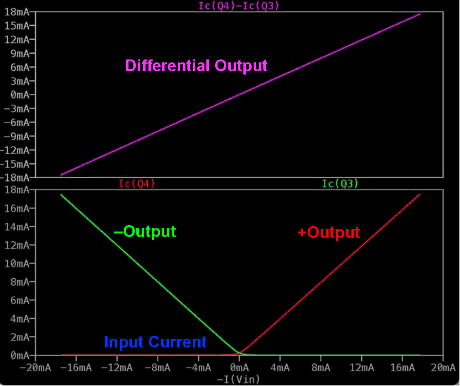
Small signal inputs
As shown in Figure 3, with smaller inputs, the circuit acts like a small signal Class A type as all the transistors operate with an IBIAS collector current. So, with zero input current, both Q1 and Q3 conduct IBIAS, as does Q2 and Q4 and the circuit acts with a differential output.
 |
|
| Figure 3. | LTspice simulation of differential output in response to small negative input current. |
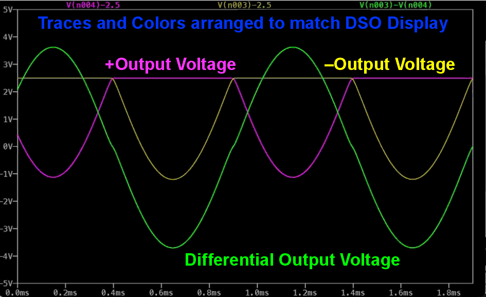
Actual results
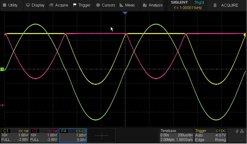 |
|
| Figure 4. | Actual results of Figure 1 schematic shown on a DSO with a sine-wave input of 2 Vpp @ 1 KHz. |
Figure 4 shows actual results from the circuit in Figure 1, shown on a DSO with a sine-wave input of 2 Vpp@1 kHz. Figure 5 shows the LTspice simulation results of Figure 1. Note the LTspice plots were set up with color and display offset bias to match DSO display for comparisons.
 |
|
| Figure 5. | LTspice simulation results of Figure 1 where the plots were set up with color and display offset bias to match. |
Also note the slight “cross over distortion” shown in both the DSO and LTspice results – common to conventional Class A/B stages. This can be improved with a higher IBIAS at the expense of higher amplifier dissipation.
This topology offers additional features other than just single-to-differential Conversion [1]. It addresses the dynamic input impedance as a function of instantaneous input signal level; an area often not addressed in conventional amplifier discussions.
Signal induced distortion begins with the effective amplifier input impedance changing with dynamic signal level and working against the source impedance creating a non-linear signal dependent voltage/power divider which modulates the input signal level.
Improving input impedance
Figure 6 shows a version where additional resistors are added to improve the input impedance variation with input signal level [2]. Note the inclusion of additional resistors to help balance the input impedance variations over large input signal swings while still maintaining an equal collector current bias for each device as determined by IBIAS.
 |
|
| Figure 6. | A high dynamic range amplifier with additional resistors to help balance the input impedance variations over large input signal swings while still maintaining an equal collector current bias for each device as determined by IBIAS. |
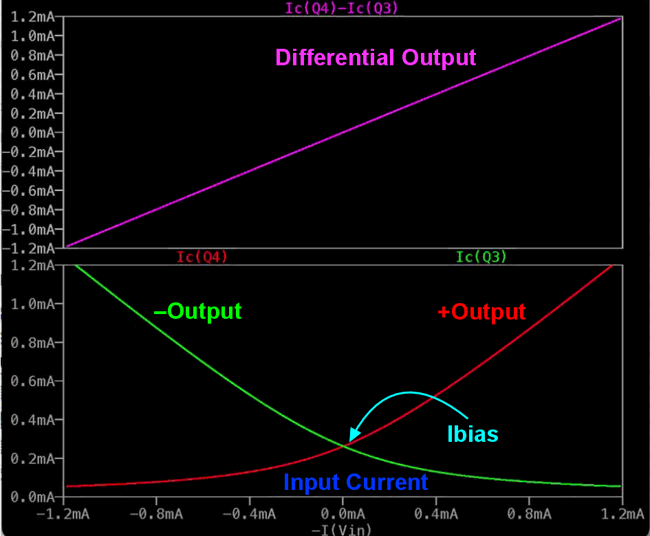
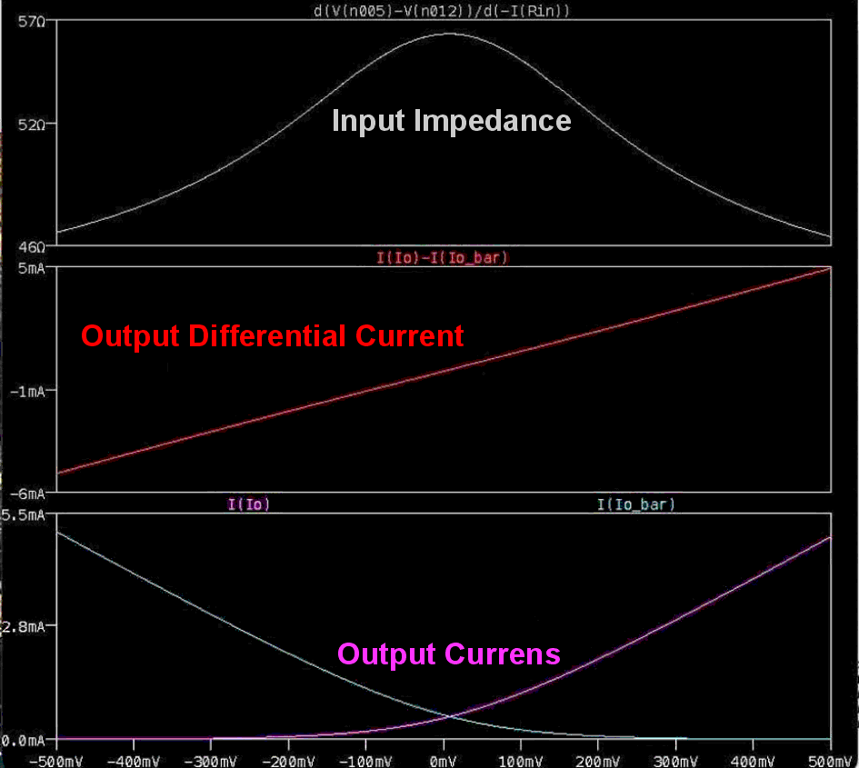
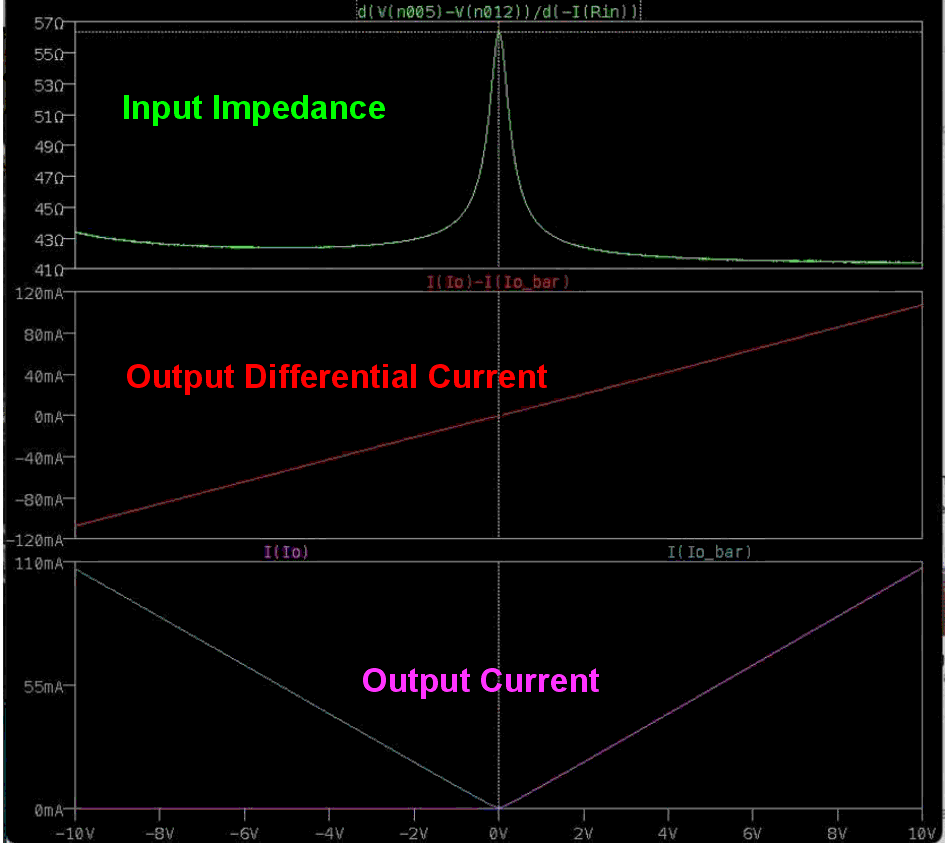
As shown in Figure 7 and Figure 8, the LTspice input impedance results were created by taking the derivative of input voltage with respect to input current as the input is swept across a large positive and negative range.
 |
|
| Figure .7 | Small signal input impedance results and output differential current. |
 |
|
| Figure 8. | Large signal ±10 V peak input impedance results and output differential current. |
High bandwidth and dynamic range single-to-differential amplifier circuit
These circuits operate in the “current domain” and can offer very high bandwidths with high dynamic range at low static power dissipation from a single supply. In the distant past, the author has implemented this with high frequency SiGe bipolar transistors in a BiCMOS process with good results.
References
- B. Gilbert, “The MICROMIXER: a highly linear variant of the Gilbert mixer using a bisymmetric Class-AB input stage,” in IEEE Journal of Solid-State Circuits, vol. 32, no. 9, pp. 1412-1423, Sept. 1997, doi: 10.1109/4.628753.
- Interesting Amplifier Topology