Miguel Usach Merino, Analog Devices
Digital potentiometers (digiPOTs) provide a convenient way to adjust the ac or dc voltage or current output of sensors, power supplies, or other devices that require some type of calibration – with timing, frequency, contrast, brightness, gain, and offset adjustment being just a few of the possibilities. Digital setting avoids virtually all of the problems associated with mechanical potentiometers, such as physical size, mechanical wear out, wiper contamination, resistance drift, and sensitivity to vibration, temperature, and humidity – and eliminates layout inflexibility resulting from the need for screwdriver access.
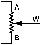
The digiPOT can be used in two different modes: potentiometer or rheostat. In potentiometer mode, shown in Figure 1, three terminals are available; the signal is connected across Terminals A and B, while Terminal W (as in wiper) provides the attenuated output voltage. When the digital ratio-control input is all zeros, the wiper is typically connected to Terminal B.
 |
|
| Figure 1. | Potentiometer mode. |
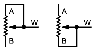
When the wiper is hardwired to either end, the potentiometer becomes a simple variable resistor, or rheostat, as shown in Figure 2. The rheostat mode permits a smaller form factor, since fewer external pins are required. Some digiPOTs are available only as rheostats.
 |
|
| Figure 2. | Rheostat mode. |
There are no restrictions on the polarity of currents or voltages appearing at the digiPOT resistance terminals, but the amplitude of ac signals cannot exceed the power-supply rails (VDD and VSS) – and the maximum current, or current density, should be limited when the part is operated in rheostat mode, especially at lower resistance settings.
Typical Applications
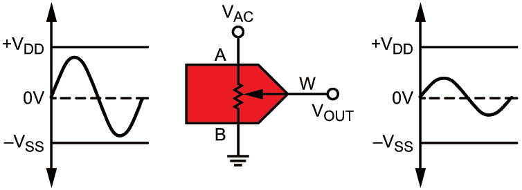
Signal attenuation is inherent in potentiometer mode, for the device is basically a voltage divider. The output signal is defined as:
VOUT = VIN × (RDAC/RPOT),
where RPOT is the nominal end-to-end resistance of the digiPOT, and RDAC is the digitally selected resistance between W and the reference pin of the input signal, typically Terminal B, as shown in Figure 3.
 |
|
| Figure 3. | Signal attenuator. |
Signal amplification requires an active component, typically an inverting or noninverting amplifier. Either potentiometer or rheostat mode can be used, with the appropriate gain equation.
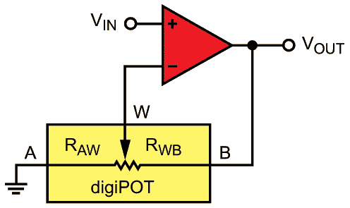
Figure 4 shows a noninverting amplifier using the device as a potentiometer to adjust the gain via feedback. Since the fraction of output fed back, RAW/(RWB + RAW), must be equal to the input, the idealized gain is
![]()
The gain of this circuit, inversely proportional to RAW, increases rapidly as RAW approaches zero, defining a hyperbolic transfer function. To limit the maximum gain, insert a resistor in series with RAW (and in the denominator of the gain equation).
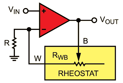
If a linear gain relationship is desired, the rheostat mode can be used in conjunction with a fixed external resistor, as shown in Figure 5; the gain is now defined as:
![]()
For best performance, connect the lower capacitance terminal (the W pin in newer devices) to the op-amp input.
Advantages of digiPOTs for Signal Amplification
The circuits shown in Figure 4 and Figure 5 have high input impedance and low output impedance, and can work with unipolar and bipolar signals. digiPOTs can be used in vernier operation to provide greater resolution over a reduced range with fixed external resistors, and can be used in op-amp circuits with or without signal inversion. In addition, they have low temperature coefficients – typically 5 ppm/°C in potentiometer mode and 35 ppm/°C in rheostat mode.
 |
|
| Figure 4. | Noninverting amplifier in potentiometer mode. |
 |
|
| Figure 5. | Noninverting amplifier in rheostat mode. |
Limitations of digiPOTs for Signal Amplification
When handling an ac signal, digiPOT performance is limited by bandwidth and distortion. Bandwidth is the maximum frequency that can pass through the digiPOT with less than 3-dB attenuation due to parasitic components. Total harmonic distortion (THD) – here defined as the ratio of the rms sum of the next four harmonics to the fundamental value of the output – is a measure of signal degradation as it passes through the device. The performance limits implied by these specifications are caused by the internal digiPOT architecture. An analysis will be helpful in order to fully understand these specifications and reduce their negative effects.
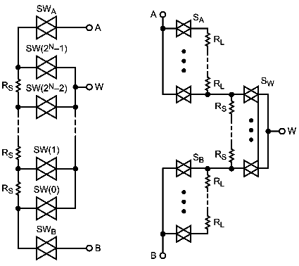
The internal architecture has evolved from the classical serial resistor array, shown in Figure 6a, to the segmented architecture, shown in 6b. The main improvement is the decreased number of internal switches required. In the first case, a serial topology, the number of switches is N = 2n, where n is the resolution in bits. With n = 10, 1024 switches are required.
 |
|
| Figure 6. | a) Convention3al architecture. b) Segmented architecture. |
The proprietary (patented) segmented architecture uses a cascade connection that minimizes the total number of switches. The example of Figure 6b shows a two-segment architecture, formed by two types of blocks: MSB on the left, and LSB on the right.
The upper and lower blocks at left are strings of switches for the coarse bits (MSB segment). The block at right is a string of switches for the fine bits (LSB segment). The MSB switches establish a coarse approximation to the RA/RB ratio. Because the total resistance of the LSB string is equal to a single resistive element in the MSB strings, the LSB switches establish the fine portion of the ratio at any point of the main string. The A and B MSB switches are complementary coded.
The number of switches in the segmented architecture is:
N = 2m + 1 + 2n – m,
where n is the total number of bits and m the number of bits of resolution in the MSB word. For example, if n = 10 and m = 5, 96 switches are required.
The segmented scheme requires fewer switches than the conventional string:
Difference = 2n – (2m + 1 + 2n – m)
In this example, the savings would be
1024 – 96 = 928!
In both architectures, switches are responsible for choosing among the different resistance values, making it important to understand the ac error sources in an analog switch. These CMOS (complementary-metal-oxide semiconductor) switches are made up of P-channel and N-channel MOSFETs in parallel. This basic bilateral switch maintains a fairly constant resistance (RON) for signals up to the full supply rails.
Part 2 here
