Barry Hoberman
Electronic Design
Among the next-generation memory technologies, spin-torque MRAM holds great promise due to its persistence, speed, and cost-effectiveness, but misconceptions surround it nonetheless
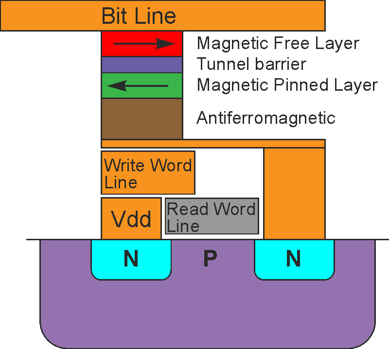
Spin-torque magnetoresistive random access memory (ST-MRAM) is emerging as the most promising of the next-generation memory technologies. ST-MRAM is persistent, as a result of storing data when the power is off. It’s fast, reading and writing at DRAM and even SRAM cache speeds. On top of that, the memory is cost-effective – it uses a small single-transistor bit-cell and requires only two or three additional masking steps.

MRAM does have its own peculiarities, though. Let’s examine some of the most common misconceptions or myths about MRAM.
1. Writing an ST-MRAM is 100% predictable and deterministic.
You might think so. After all, if you write a good SRAM or DRAM memory cell one trillion times, barring soft errors or some external event, the cell will be correctly written one trillion times. However, MRAM is different because setting a magnetic polarization vector is a probabilistic event – writing an MRAM cell one trillion times will mostly work, but very occasionally may not. One of the biggest challenges with MRAM technology is making the write error rate (WER) as low as possible, and also compensating for the few errors that will occur.
2. I’ve seen very impressive MRAM speed specs quoted. With speeds of 2 to 3 ns, it looks like it can fully replace SRAM.
MRAM specs can be optimized. For example, increasing the write voltage improves both the switching time and the WER described previously. But, there’s a downside. Greater voltage significantly increases power and reduces endurance – the number of write cycles before the tunnel barrier wears out. Like all memory designs, the key to MRAM design is to find the right blend of speed, power, endurance, and retention to meet the application requirement.
The ST-MRAMs are showing great promise in this regard. They’re persistent by storing data when the power is off. They’re also fast – they can read and write at DRAM and even SRAM cache speeds. Lastly, they’re cost-effective, using a small single-transistor bit-cell and requiring only two to three additional masking steps.
3. MRAMs today are just like the core memories from decades ago, only smaller.
The category of “MRAM” includes three generations of devices. First are the original core memories and other low-density, first-generation MRAM parts that use “field-switching,” along with ST-MRAM, which comes in two flavors. The second-generation MRAM is “in-plane,” where the magnetic polarization vectors are parallel with the plane of the magnetic layer (i.e., wafer surface). The third-generation MRAM is “perpendicular,” in which the vector is perpendicular to the plane of the wafer. All mainstream MRAM activities today are focused on perpendicular magnetic-tunnel-junction (MTJ) devices.
4. MRAMs are quite power hungry.
In fact, MRAMs are extremely low power. For instance, compared to flash memory, ST-MRAMs use 1,000X to 10,000X less energy to write a bit of data, making them the ideal low-energy memory for IoT devices. For SRAM-type applications, MRAMs don’t consume leakage power while retaining data. So, for DRAM-type applications, they have neither leakage power nor refresh power – a significant savings.

5. MRAM is the most complex of all of the next-generation memory technologies.
Each of the emerging memory technologies has characteristics that are complex, and certainly the last few points have made it seem that MRAM is complex, too. The probabilistic nature of MRAM is challenging to deal with, and some companies still struggle to completely eliminate bit errors.

Yet, compared to other next-generation memories, MRAM principles are far more widely studied and commercialized because the technology came from the disk-drive industry: The MTJ of a read head is similar to the MTJ in an in-plane MRAM bit-cell. Many hundreds of millions are made and incorporated into rotating disk drives every year. And perhaps most important, all of the physical materials are static in an MRAM. Atoms don’t have to move, as in an RRAM, nor do the materials have to change state, as in a phase-change RAM.
6. MRAMs are the ultimate memory – the speed of SRAM cache with the retention of flash.
This statement is true if each piece is addressed separately, because retention and writing speed are in tension – increasing one tends to degrade the other. It’s also true that MRAM can meet, or exceed, flash retention specs and be orders of magnitude more durable, faster, and lower power. In addition, while an MRAM device can execute at cache speeds, the flash-like MRAM will be several times slower, perhaps 40- to 100-ns write times. Meanwhile, the sub-10-ns MRAM cache will be challenged in conventional ST-MRAM technology to have retention time greater than seconds or perhaps hours.
7. MRAM manufacturing is very complex.
MRAM manufacturing steps are actually quite straightforward: Deposit the materials stack, etch it, and connect it. The challenge, of course, is developing the materials stack and etching process for high-density MRAM. But once achieved, MRAM manufacturing has small incremental cost over CMOS with only two to three added masking steps, plus related processing.
8. I see people talking about various diameter MTJs. I think the MTJ diameter should match the process node I’m using.
MTJ diameter is loosely related to process node. The MTJ must be small enough to fit within the pitch of the underlying process, but this pitch is generally much larger than the process node itself. For example, a 28-nm logic process will most likely use MTJs that are 40 to 60 nm in diameter. Selecting the MTJ diameter is actually quite complex, since many MTJ attributes change as the device gets smaller.
9. MRAM manufacturing equipment comes from the disk-drive industry and isn’t appropriate for semiconductor high-volume manufacturing.
Today, TEL, Applied Materials, the Anelva division of Canon, Singulus, LAM, and others are all developing or shipping tools for high-throughput 300-mm MRAM manufacturing.
10. Magnetic fields emanating from an MRAM will disturb underlying CMOS, as well as magnetic sensors and compasses in mobile devices.
The field from the small MTJ pillar falls off very rapidly and is negligible at the depth of the transistor.

11. MRAM memories have some form of data loss that’s worse than SRAM.
SRAM and DRAM have always been subject to data loss due to the impact of background ionizing radiation. This problem gets much worse as lithography advances to address today’s feature sizes. The MRAM MTJ storage device is inherently immune to data loss from ionizing radiation. Therefore, MRAM technology, when coupled with appropriate CMOS technology, is ideal for aerospace applications and other areas where radiation is present.
