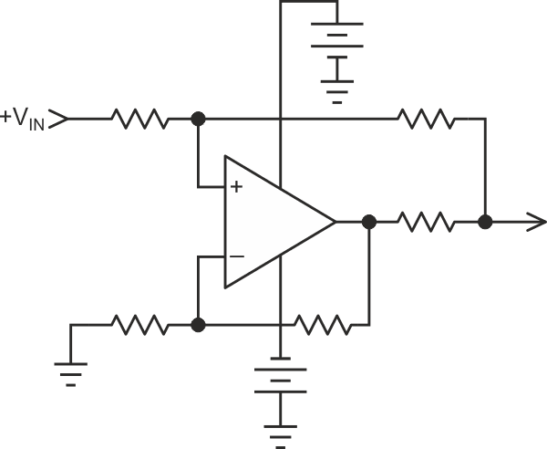
A bi-directional current source for a grounded load will always have some complication in its construction. The improved Howland Current Pump as shown in Figure 1 is the most frequent choice for this function. The Howland requires carefully matched resistors or resistor networks. Alternatively, you can use precision difference amplifiers although some trim may still be required to get the necessary performance.
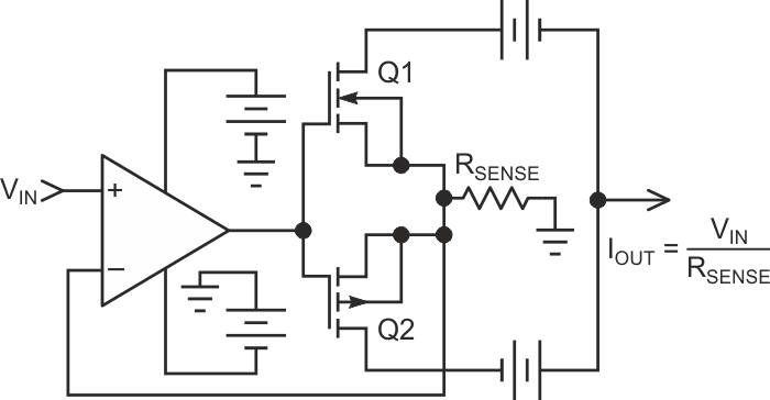
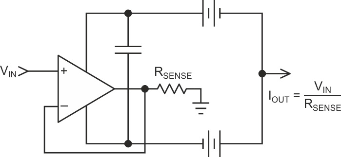
The circuit shown in Figure 2, which for the purposes of this article we'll call the Simple Source, accomplishes the same function with only one precision resistor. It was pointed out in the first paragraph that there is always some complication. In this case you'll need to add an isolated dual power supply, which is readily and inexpensively found.
The circuit shown in Figure 2 depicts what looks like an op amp with a simple MOSFET (you can use bipolar if you wish) buffer on the output. Feedback is taken from the MOSFET sources from a grounded resistor. You'll note this is starting to resemble the classic uni-directional op amp/MOSFET combination used to provide a current source. The only complication is the need for the floating power supplies(s) on the MOSFET drains with the output taken from the center tap of the supplies. Gain accuracy is mainly a function of the single current sense resistor when the op amp is operated in a unity gain configuration (gain can be taken although you add two more resistors to the accuracy equation).
Along with the accuracy benefit, this circuit provides better frequency response with inductive loads since the load is not within the feedback loop as it is with the Howland. The (mostly) unilateral transfer function of the output MOSFET isolates the loop from the load, at least until the dynamic range is exceeded. By comparison the improved Howland can require heavy compensation with inductive loads with an accompanying reduction in bandwidth.
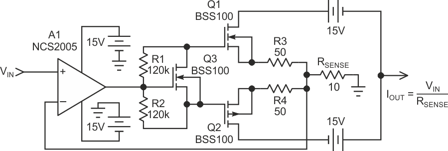
Note that the simplified circuit of Figure 2 lacks Class A/B biasing for the MOSFET's. This may not be a problem for DC or low frequency applications. The actual circuit tested in Figure 3 includes a VGS multiplier configuration that adds a MOSFET and a pair of resistors for Class A/B biasing to eliminate crossover distortion since it would be used to test transient response.
Test results
A test of the Howland for accuracy would not be fair since Howland accuracy is proportional to the lengthy effort you put into it, which is exactly the point of the Simple Sources. Suffice to say that either circuit can ultimately provide high accuracy, but the task is considerably simplified with the Simple Source.
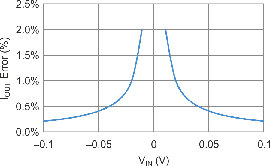
The accuracy test is a plot of output current error using a 0.1% resistor for. All testing was targeted at evaluating performance at up to ±10 mA output current. Figure 4 depicts output current error plotted against input voltage.
 |
|
| Figure 4. | Output error of the circuit in Figure 3 plotted over a range of ±10 mA. |
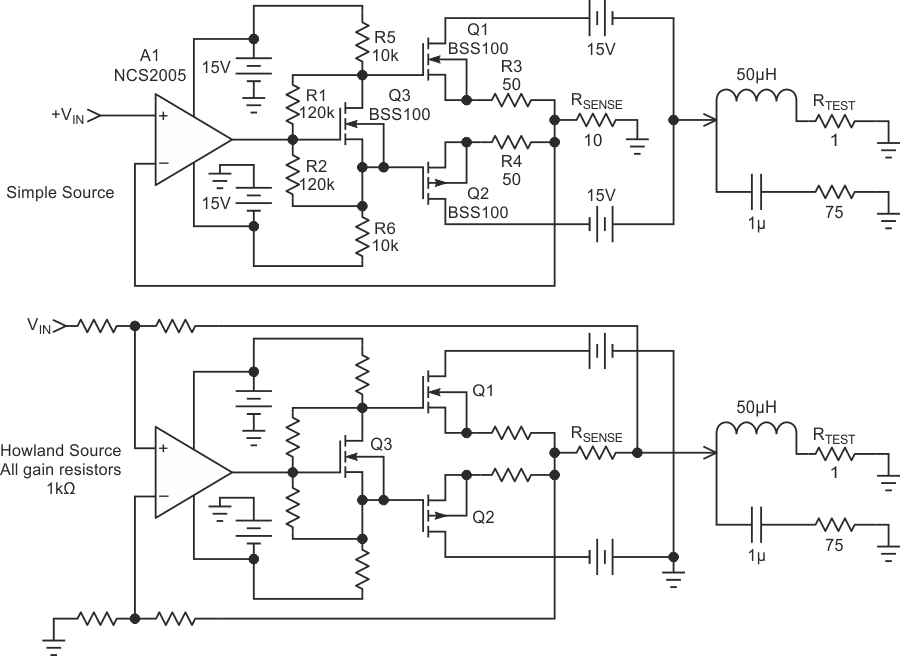
To show the benefit of this circuit when driving an inductive load it was compared to a Howland with both circuits driving a 50 µH inductor. The schematic in Figure 5 is included to show how the Simple Source was re-configured as a Howland current source. In each case the output current was observed across the 1 Ω non-inductive resistor in series with the 50 µH inductor.
 |
|
| Figure 5. | Test circuits to compare dynamic response of Simple Source (top) vs. Howland (bottom). Output signal is observed across RTEST. |
Both circuits required compensation networks across the inductor, but for different reasons. In the case of the Simple Source the output capacitance and load inductance need a snubber to control the ringing. The Howland also demonstrates ringing, much of which is caused by the inductor in the feedback loop. Using a square wave input, compensation was performed empirically. In each case start with a resistor across the inductor and reduce it until overshoot and ringing is smoothed out. Then introduce a capacitor and decrease value until overshoot and ringing start to show back up.
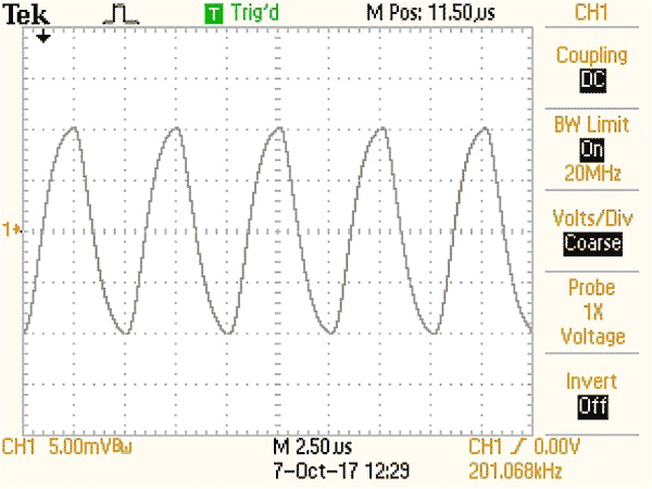
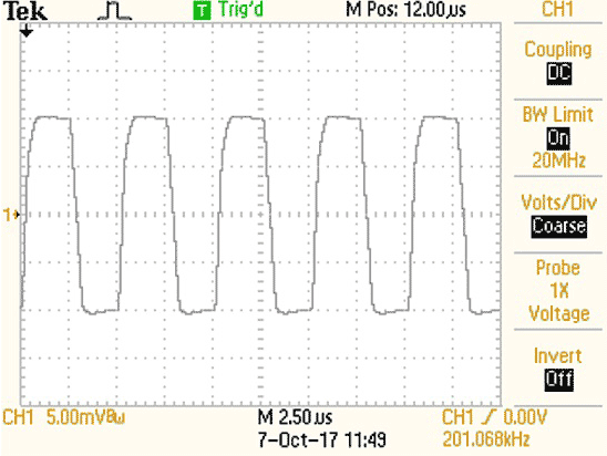
The frequency was taken as high as possible, which turned out to be 200 kHz to get a meaningful comparison. The waveform of Figure 6 for the Howland shows that this is actually beyond the limit of the Howland at this frequency.
It can get simpler
In the event that Figures 2 and 3 are more complex than you need, and you can sacrifice some performance, you can use the schematic of Figure 8 for the simplest possible approach. Among the obvious considerations at first glance is that you are now moving the op amp power supply pins to generate the output with obvious dynamic range limitations by the minimum power supply rating of the op amp. Quiescent current flows from rail-to-rail with little effect on output accuracy when CMOS op amps are used, but expect several percent of error with bipolar op amps. Bypassing can be a concern although rail-to-rail bypassing can be used. The author has used this circuit for some time as a current output adapter from a network analyzer for measuring output impedance of op amps. It hasn't been tested over a wide variety of op amps, while many will work fine here, there will be op amps that won't work well for this circuit.
A caution on simulating this circuit. Not all op amp spice models correctly model the flow of load current in the power supply pins, an essential behavior to simulating this circuit.
