Despite massive, large-scale integration being ubiquitous in contemporary electronic design, discrete MOSFETs in the classic CMOS totem pole topology are still sometimes indispensable. This makes tips and tricks for driving them efficiently with logic level signals likewise useful, because it can be a “bit” tricky, especially if other than standard logic voltage levels are involved.
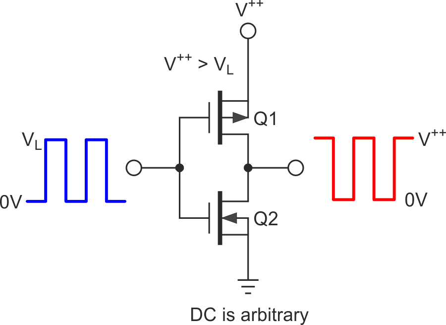
If (happily) they are not, we have Figure 1.
 |
|
| Figure 1. | The simplest case of logic signal totem pole drive – direct connection works if V++ <= VL. |
In the lucky circumstance that the totem FET source pins are connected to positive and negative rails that match the logic levels, a simple direct connection (a wire) will suffice. All that’s needed for success then is that:
- The FET ON/OFF gate-source voltage level lies within the logic signal excursion, and
- The logic signal source has sufficient drive to cope with the paralleled FET input capacitances.
Item 2 is particularly important, because it affects the archenemy of totem pole efficiency, cross-conduction.
It often happens that, during the transition between Q1-conducting and Q2-not to the opposite state, there will be an interval of overlap when both transistors conduct. This is “cross-conduction”, and it wastes power, sometimes a lot. The longer its duration, the greater the waste. The duration of cross-conduction depends on the time required for the logic signal to complete the 0/1 or 1/0 transition, which depends on how long it takes to charge and discharge the respective gate input capacitances. The cross-conduction gremlin is somewhat mitigated by the fact the capacitance that delays one FET’s turn-off also delays its complementary partner’s turn-on, but speed is still vital.
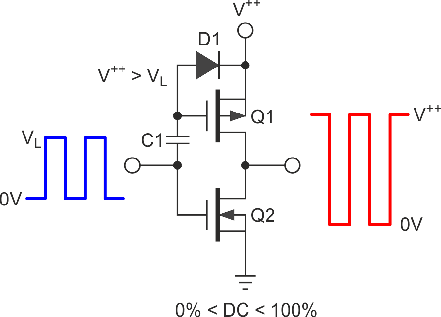
Now suppose Q1’s V++ source voltage is higher than VL. What now? Figure 2 shows a simple solution: AC coupling.
 |
|
| Figure 2. | AC coupling can solve the problem of positive rail voltage mismatch if the control signal runs continuously. |
Of course, this simple fix will only work if the logic signal can be relied upon to always have an AC component. That is to say, if only its duty cycle is never 0% (always OFF) nor 100% (always ON): 0% < DC < 100%. C1 should have at least an order of magnitude greater capacitance than Q1’s gate capacitance (e.g., 1 nF). While D1 can usually be an ordinary junction diode (e.g., 1N4148), a Schottky type can be a better choice if a few extra hundreds of mV of gate drive are needed.
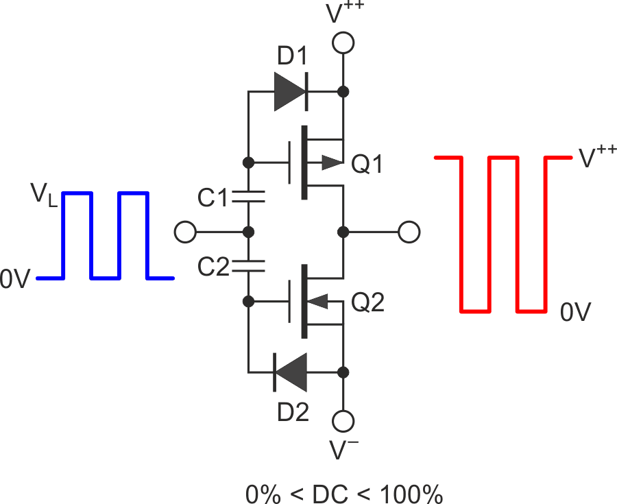
AC coupling can also come to the rescue if the totem’s negative rail is below ground, as shown in Figure 3. The same DC limitation applying, of course.
 |
|
| Figure 3. | Ditto for AC coupling and negative rail mismatch, too. |
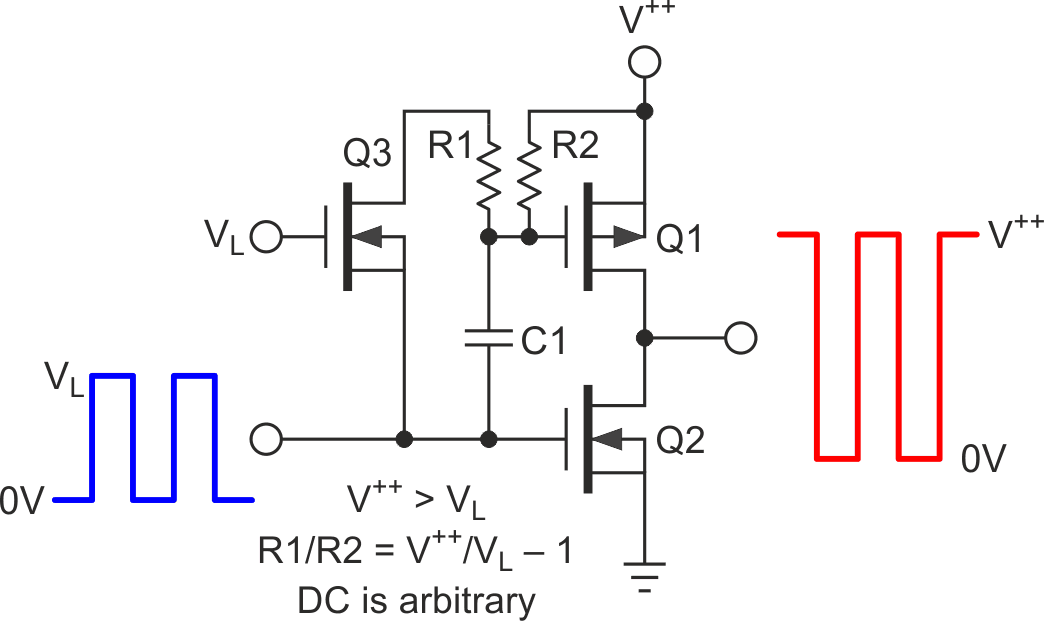
So, what to do if DC doesn’t obey the rules, and we can’t rely on a simple diode to define signal levels? See Figure 4.
 |
|
| Figure 4. | “Grounded” gate Q3 maintains C1 charge when logic signal stops. |
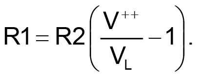
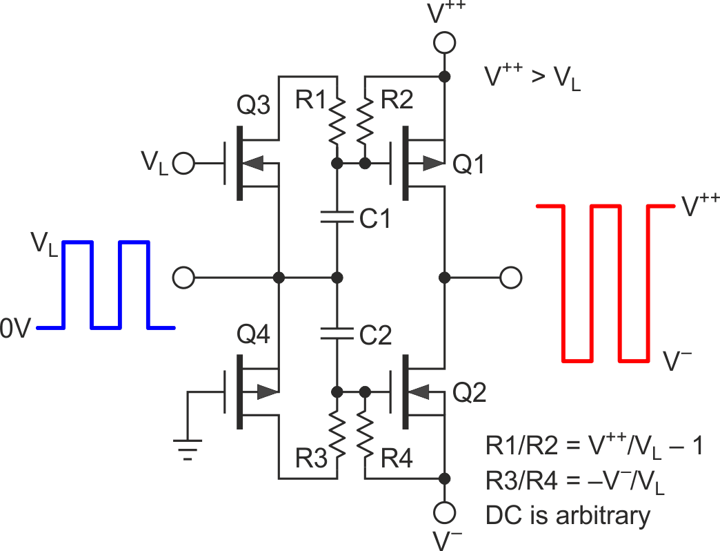
Small-signal transistor Q3’s configuration as a common-gate, non-inverting high-speed amplifier transfers necessary steady-state current to Q1. Choose R2 to be a low enough resistance to source Q2’s maximum expected source-to-gate leakage current (R2 = 10k will typically be a very conservative choice), then
And of course, as illustrated in Figure 5, the same trick works for a negative totem rail.
 |
|
| Figure 5. | Grounded gate Q4 shifts logic signal to negative rail referred C2 and Q2. |