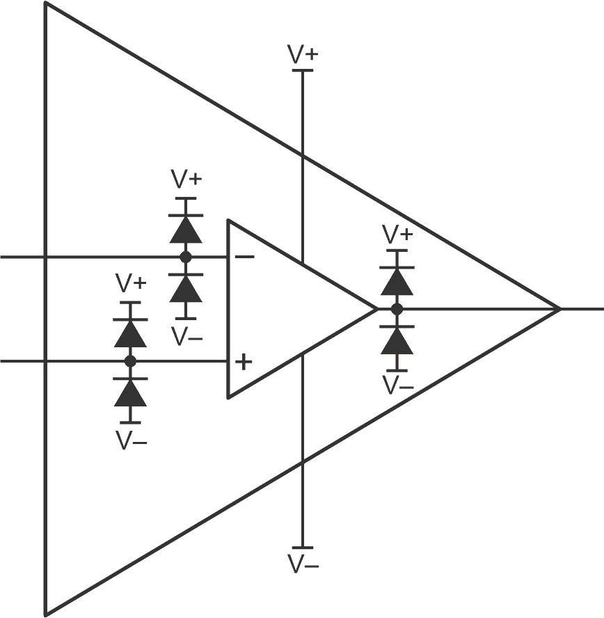
Most operational amplifiers (op amps) have input and output electrostatic discharge (ESD) protection diodes, as shown in Figure 1. These diodes are designed for protection from ESD damage during device testing and product assembly.
 |
|
| Figure 1. | Op amps have input and output ESD protection diodes. |
An ESD event can drive a very high current into the ESD diode, but only for nanoseconds. And while ESD diodes are designed to withstand ESD pulse, electrical overstress events of longer durations will require additional external components. Most input ESD protection diodes are designed to withstand 10 mA of continuous current, but electrical overstress faults often cause current well beyond the 10-mA limit.
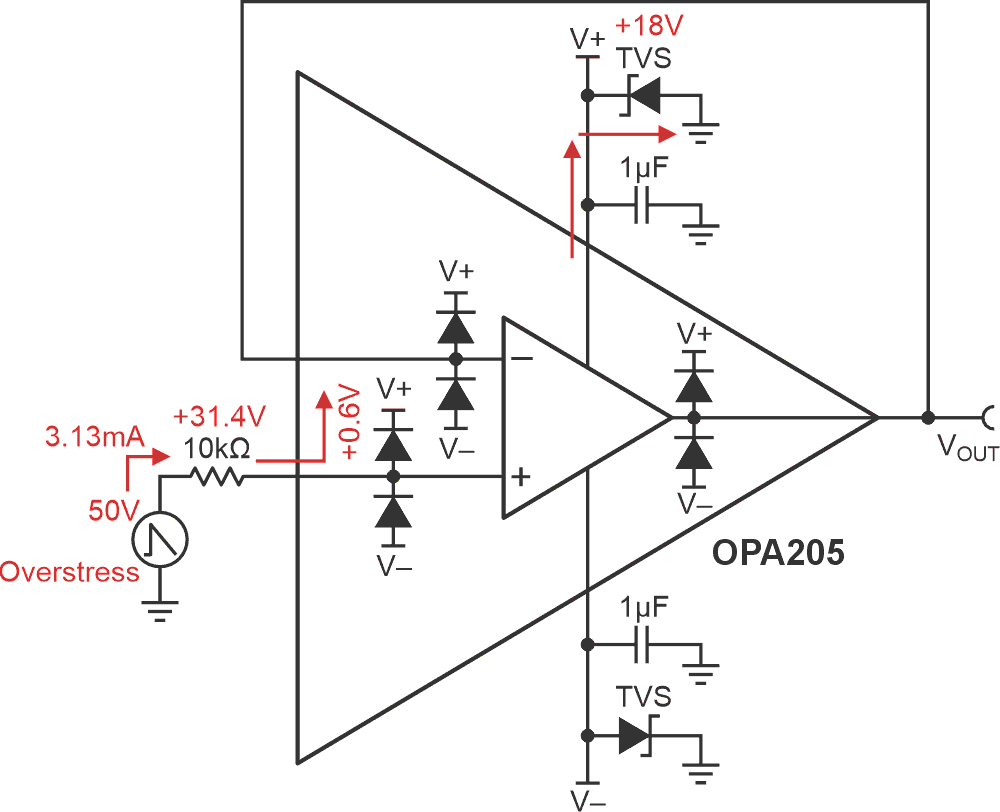
One common approach used to limit op-amp input overstress current is to simply add an input current-limiting resistor and a transient voltage suppressor (TVS) diode on each supply (Figure 2). The resistor will limit the input current, but some of the overstress voltage will still be directed onto the power supply. The TVS diode will protect the power supply from the overstress voltage channeled through the ESD diodes.
 |
|
| Figure 2. | The electrical overstress (EOS) protection scheme shown uses the OPA205 precision op amp. |
You need a TVS diode because many voltage regulators do not have the ability to sink current, nor can they respond fast enough to protect the supply. The resistance value required to protect the op amp depends on the magnitude of the overstress signal on the input. Large overstress signals will require large resistances.
The example in Figure 2 uses a 10-kΩ resistor to limit the current to a safe level of 3.13 mA for a 50 V overstress signal. Using the protection scheme in Figure 2 can be very effective but does have a few limitations.
The resistor will introduce a DC offset error because of the op-amp input bias current (IB). This error will add directly to the input offset voltage (VOS) of the op amp and limit the circuit’s DC accuracy. Another limitation of the resistive input protection is that resistors generate thermal noise. Equation 1 calculates the noise, enRin, density as:
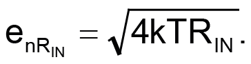 |
(1) |
You should then compare this noise to the op-amp noise spectral density specification.
In the example shown in Figure 2, the input noise specification is 7.2 nV/√Hz and the resistor generates 12.8 nV/√Hz. Thus, the overall noise will be dominated by the protection resistor and will be much higher than the noise of the op amp alone.
 |
(2) |
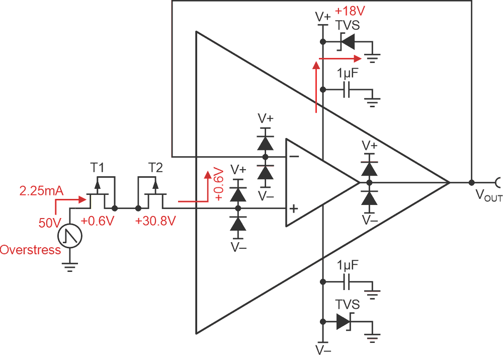
The junction field-effect transistor (JFET) input protection scheme shown in Figure 3 is an approach that enables reliable input protection while minimizing errors from IB and resistor noise. The JFET circuit has low resistance when no current flows through it, but the resistance rapidly increases when current does flow through it.
 |
|
| Figure 3. | The JFET input protection shows the circuit operation under fault condition. |
Thus, in normal operating conditions, the JFET circuit will have low resistance and add minimal noise and IB error. Under a fault condition, the JFET device will rapidly increase, which will limit current and protect the circuit. When the fault is removed, the JFET will return to its normal low impedance state.
You can build this kind of JFET circuit using discrete JFETs, but it’s also integrated into some amplifiers. In general, when you see the term “input-overvoltage-protected” in amplifier datasheets, the protection is JFET input protection. Using integrated protection will save PCB area, save design effort, and generally reduce overall costs.
Review of JFET fundamentals
In order to understand JFET protection, let’s review some JFET fundamentals. This article will focus on P-channel JFET devices, but the same approach applies to N-channel devices with the polarities reversed. You can think of the JFET transistor as a voltage-controlled resistance, where the channel resistance is controlled by the voltage gate-to-source (VGS) and the voltage drain-to-source (VDS).
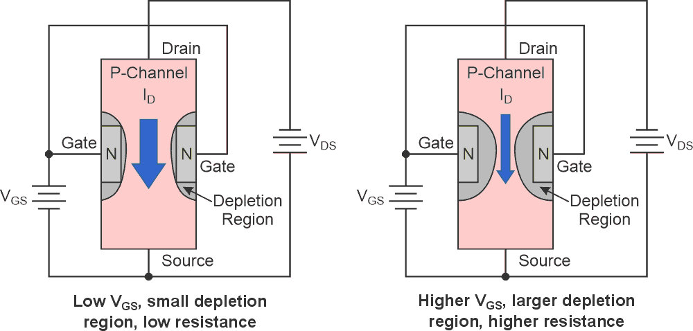
It’s important to understand that the JFET operates in depletion mode. The gate-to-source junction is reverse-biased, which creates a depletion region that restricts channel current flow (ID). Increasing the reverse bias voltage will increase the depletion region, which increases the channel resistance. The lowest resistance happens when VGS = 0 V, which has a very small depletion region, as shown in Figure 4.
 |
|
| Figure 4. | Here is a comparison between resistance region versus depletion region. |
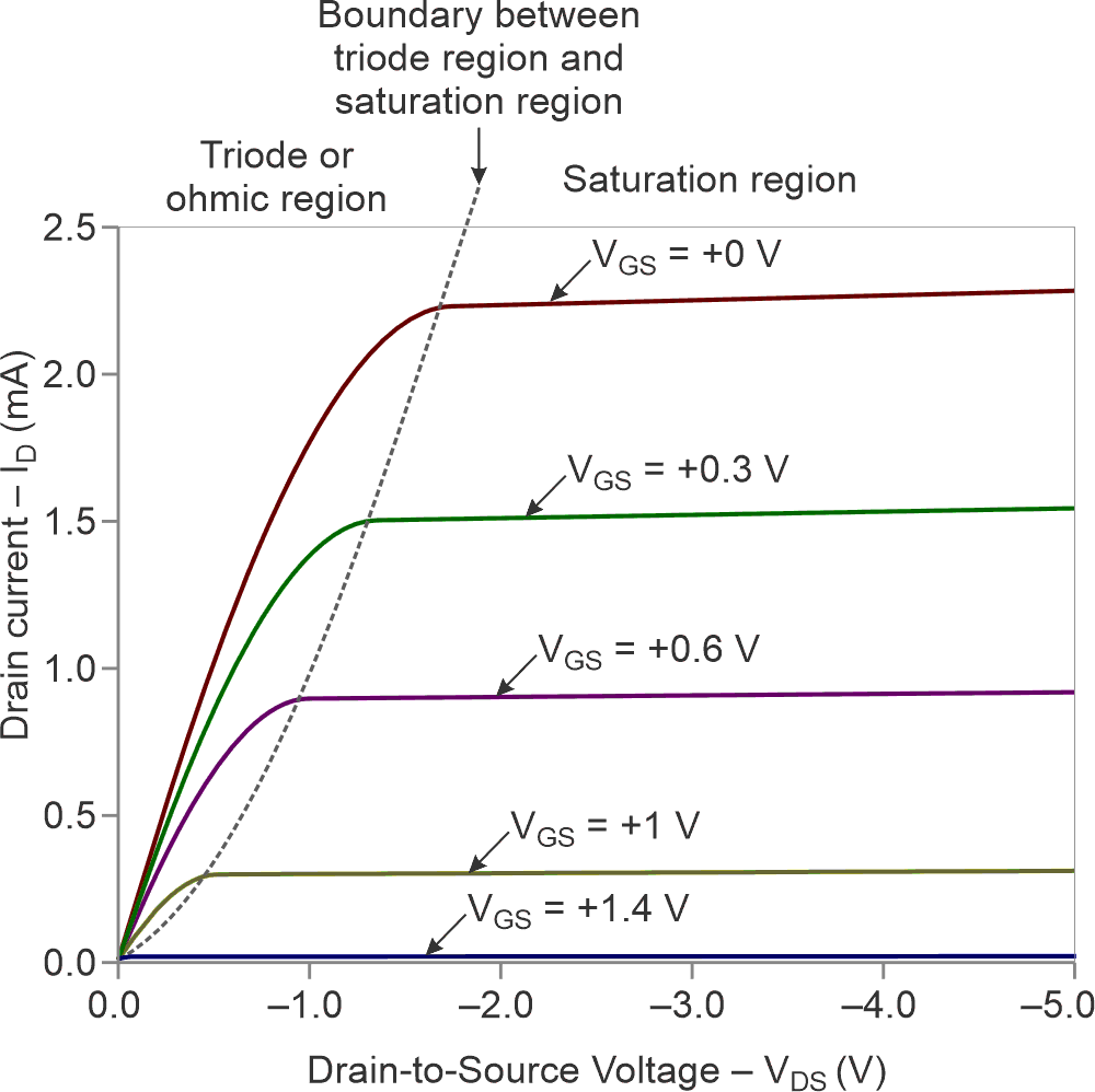
Adjusting VDS will also affect the depletion region. For a lower VDS, the channel acts like a resistor, and the transistor is said to be in its ohmic region or triode region. In the ohmic region, an increase in VDS will cause a proportionate increase in drain current (ID), just as you would see on a resistor (see the left-hand side of Figure 5).
 |
|
| Figure 5. | See P-channel JFET characteristic curve highlighting ohmic and saturation regions. |
For a higher VDS, the channel pinches off and the transistor is said to be in the saturation region. While in the saturation region, the current through the transistor is held relatively constant for a wide range of drain-to-source voltage (see the right-hand side of Figure 5).
As mentioned earlier, for a JFET, the gate-to-source junction is normally reverse-biased. When forward biased, the JFET will no longer act like a transistor, and the curves in Figure 5 no longer apply. In this case, the JFET will act as a normal PN junction diode with a forward voltage drop of about 0.6 V, with current limited by external components.
Generally, it’s best to avoid the forward-bias mode of operation, but in the case of the input protection circuit, one of the transistors will become forward-biased in the presence of overstress signals.
Operation of the JFET protection circuit
The JFET input protection in Figure 3 shows the circuit operation under fault condition. This example applies a +50 V input fault to an op amp with ±18 V power supplies. Transistor T1 acts as a forward-bias diode, and T2 acts as a JFET in the saturation region, with VGS = 0 V.
Assuming that the transistors in the protection circuit use the I-V curve shown in Figure 5, ID is limited to approximately 2.25 mA when VGS = 0 V and VDS > –1.5 V (the saturation region). Thus, the JFET circuit protects the op amp from damage because it limits the input current to less than the 10-mA absolute maximum current specification. The current flow with VGS = 0 V is defined as IDSS, so IDSS < 10 mA is required for op-amp input protection.
A –50 V input fault would have the same effect, except that T2 would be a forward-bias diode and T1 would be in the saturation region. During the fault condition, the JFET will act as a current-limiting resistance where the resistance increases for larger fault voltages and maintains a constant current <10 mA.
During normal operation, both JFET transistors will be in the ohmic region and have relatively low resistance. Furthermore, during normal operation, the current flow through the JFET will be the op-amp input bias current (the range is typically femtoamperes to nanoamperes). You can graphically estimate the ohmic-region resistance by looking at the slope of the ID curve with VGS = 0 V.
For the transistor specified in Figure 5, the ohmic-region resistance is approximately 500 Ω (RDS = 1 V/2 mA = 500 Ω). Conversely, under the fault condition shown in Figure 3, the JFET is in the saturation region and its resistance is approximately 13.7 kΩ.
The important point is that under normal operating conditions, the JFET resistance is small; consequently, the thermal noise will be low ( for 500 Ω). Under a fault condition the resistance is high, but in this case the thermal noise is not important, since the amplifier is not functioning normally, and the resistor only needs to protect the op amp from damage.
Selecting JFETs for a discrete protection circuit
Some op amps, such as the OPA206, incorporate a JFET protection circuit into the device. In cases where the amplifier does not include a JFET, you may want to build your own protection circuit. If thermal noise or bias-current-induced offset are a concern, you may want to use a JFET protection circuit. If noise and IB error are not a concern, you can simply use a large input protection resistor, as shown in Figure 2.
Assuming that you want JFET input protection, you should confirm that the maximum drain-to-source saturation current (IDSS) is <10 mA so that the JFET sufficiently limits the input current during a fault condition. Also, since one of the two JFET transistors will have a forward-bias gate-to-source junction, you must confirm that the absolute maximum forward gate current is less than IDSS (IGF < IDSS).
Make sure not to exceed the absolute maximum drain-to-gate and source-to-gate voltage. Finally, calculate the ohmic-region resistance with VGS = 0 V to confirm that the resistance under nonfault conditions is acceptable from an error perspective.
Cost and specification impact
To understand the additional cost and specification difference between an op amp with and without an integrated JFET protection circuit, let’s compare the OPA205 chip to the OPA206 chip. Both devices use the exact same op amp, but OPA206 incorporates additional JFET protection. In reviewing the specifications for the two devices, the main difference is in the input noise and electrical overstress specifications.
The noise for OPA205 is VN = 7.2 nV/√Hz, and the noise for OPA206 is VN = 8 nV/√Hz. There is some degradation in noise, but it’s substantially less than what would be introduced by a large current-limiting resistor. The protection circuit allows OPA206 absolute maximum rating up to 40 V beyond the supply rails, but OPA205 only allows 0.5 V beyond the supply rails without external protection. OPA206 is priced about $0.07 higher than OPA205 to account for the additional circuitry.
To implement a JFET circuit discretely, you would need to purchase two JFET transistors. Typically, this would be two SOT-23 devices, which would consume about the same PCB area as the op amp itself. Furthermore, the cost of the two devices would likely exceed the cost of the additional protection in the integrated solution.
Thus, in general, it’s best to choose the integrated option when available, opting for discrete JFET protection in cases where no integrated solution is available, and the simple resistor solution is not acceptable from a noise perspective.
Use op amp with integrated JFET input protection
The requirement for op-amp fault protection has become very common in modern analog systems. However, these systems also frequently require low noise and high DC precision, and the simple resistive input protection makes meeting this goal challenging. Using external JFET protection is a good way of getting the best of both worlds.
However, external protection adds cost and PCB area. The best solution is to use an amplifier with integrated JFET input protection as this will protect the input, maintain good performance, add minimal cost, and minimize PCB area.