Cadence
On larger designs especially, PCB design teams need fast and reliable simulation to achieve convergence. Cadence® simulation technology for PCB design offers a single, unified design environment for both simulation and PCB design. With integrated analog and event-driven digital simulation, teams benefit from improved speed without sacrificing accuracy. Using advanced analysis capabilities, designers can automatically maximize the performance of circuits.
Cadence Simulation Technology for PCB design
Cadence simulation technology for PCB design provides a full-featured analog simulator with support for digital elements to help solve virtually any design challenge – from high-frequency systems to low-power IC designs. The powerful simulation engine integrates easily with Cadence PCB schematic entry solutions, improving time to market and keeping operating costs in check. An interactive, easy-to-use graphical user interface provides complete control over the design process. Availability of resources such as models from many vendors, built-in mathematical functions, and behavioral modeling techniques make for an efficient design process. Advanced analysis features (Sensitivity, Monte Carlo, Smoke, and an optimizer with multiple engines) are built on top of the simulator to improve design performance, cost-effetiveness, and reliability.
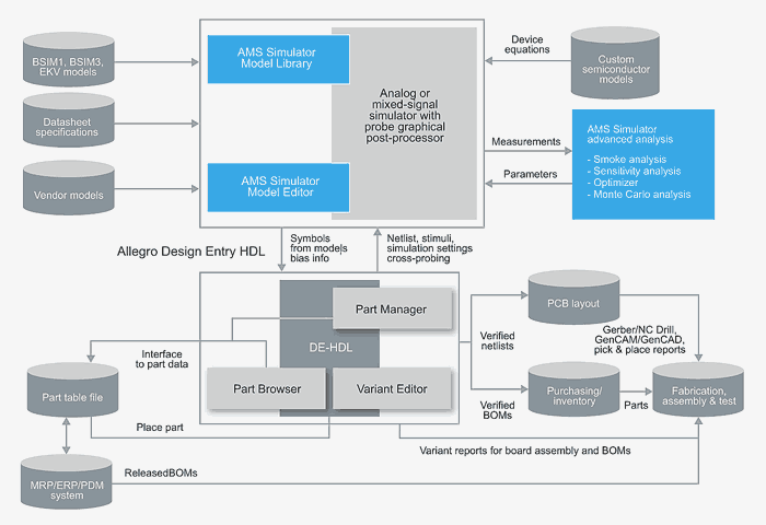
The products are tightly integrated with Cadence Allegro Design Entry HDL and Cadence OrCAD Capture. The simulation technology can also interface with MathWorks’ MATLAB Simulink package in a powerful co-simulation environment (SLPS). (See Figure 1.)
 |
|
| Figure 1. | Cadence simulation technology for PCB design. |
Benefits
- Improves simulation times, reliability, and convergence on larger designs;
- Improves speed without loss of accuracy via integrated analog and event-driven digital simulations;
- Explores circuit behavior using basic DC, AC, noise, and transient analyses;
- Allows system-level interfaces to be tested with actual electrical designs using SLPS;
- Offers library selection of more than 20,000 analog and mixed-signal models;
- Allows for automatic identification of analog and digital signals and applies A-to-D and D-to-A interfaces;
- Explores design relationships with “what if” scenarios before committing to hardware;
- Maximizes circuit performance automatically using Optimizer;
- Identifies and simulates functional blocks of complex circuitry using mathematical expressions, functions, and behavioral devices;
- Determines which components are overstressed using Smoke analysis and by observing component yields using Monte Carlo analysis.
Features
Cadence simulation technology for PCB design integrates seamlessly with the Cadence front-to-back PCB design flow, making it possible to have a single, unified design environment for both simulation and PCB design.
Design entry and editing
Select from a library of more than 18,000 symbols and models for simulation to design with Cadence PCB schematic design entry technology. It provides many features that allow you to easily capture and simulate analog designs. Both integrations include one-button simulation and cross-probing, and many other simulation utilities.
Stimulus creation
Access built-in functions that can be described parametrically or draw piecewise linear (PWL) signals freehand with the mouse to create any shape stimulus. Create digital stimuli for signals, clocks, and buses; click-and-drag to introduce and move transitions.Circuit simulationUsers can easily set up and run simulations, and then cross-probe simulation results from Probe, an industry-standard waveform viewer. Support for multiple simulation profiles enables users to recall and run different simulations on the same schematic. Simulation bias results can be viewed directly on the schematic including node voltages, device power calculations, and pin and subcircuit current. Support for Checkpoint Restart allows designers to reduce simulation times when the same circuit is simulated multiple times with minor changes.
Mixed analog/digital simulation
Integrated analog and event-driven digital simulations improve speed without loss of accuracy. A single graphical waveform analyzer displays mixed analog and digital simulation results on the same time axis. Digital functions support 5 logic levels and 64 strengths, load-dependent delays, and hazard/race checking. Allegro AMS Simulator and PSpice simulation also feature propagation modeling for digital gates and constraint checking (such as setup and hold timing).
Analog analysis
Explore circuit behavior using DC, AC, noise, transient, parameter sweeps, Monte Carlo, and DC sensitivity analyses. Allegro AMS Simulator and PSpice technology include interactive simulation controllers and two simulation solvers.
Graphical results and data display
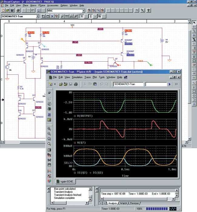
Probe Windows allows users to choose from an expanded set of mathematical functions to apply to simulation output variables. Designers can create plot window templates and use them to easily make complex measurements by simply placing markers directly on the desired pins, nets, and parts in the schematic.The tools also enable users to measure performance characteristics of a circuit using built-in measurement functions and creation of custom measurements. For data display, additional capabilities allow plotting of both real and complex functions of circuit voltage, current, and power consumption, including Bodй plots for gain and phase margin and derivatives for small-signal characteristics.(See Figure 2.)
 |
|
| Figure 2. | Cadence simulation technology for PCB design provides a complete simulation environment including simulation waveform analysis with cross-probing and bias results displayed on the schematic. |
Models
Included are a large variety of accurate internal models – which typically include temperature effects – that add flexibility to simulations. Models are available with R, L, C, and bipolar transistors plus:
- Built-in IGBTs;
- Seven MOSFET models, including industry-standard BSIM3v3.2 and the new EKV 2.6 model;
- Five GaAsFET models, including Parker-Skellern and TriQuint TOM-2, TOM-3 models;
- Nonlinear magnetic models complete with saturation and hysteresis;
- Transmission line models that incorporate delay, reflection, loss, dispersion, and crosstalk;
- Digital primitives, including bi-directional transfer gates with analog I/O models;
- Two battery models, which allow accurate simulation of the discharge cycle and operating conditions.
A device equations developer’s kit (DEDK) allows implementation of new internal model equations that can be used with Allegro AMS Simulator and PSpice simulation.
Model library
Users can select from more than 18.000 analog and mixed-signal models of devices made in North America, Japan, and Europe. Also included are more than 4,500 parameterized models for BJTs, JFETs, MOSFETs, IGBTs, SCRs, magnetic cores and toroids, power diodes and bridges, operational amplifiers, optocouplers, regulators, PWM controllers, multipliers, timers, and sample-and-holds.
Model editing
It’s easy to extract a model of a supported device type – simply enter the required data from the device’s datasheet.
Behavioral modeling
Functional blocks are described using mathematical expressions and functions, which allows designers to leverage a full set of mathematical operators, nonlinear functions, and filters. Circuit behavior can be defined in the time or frequency domain, by formula (including Laplace transforms), or by look-up tables. Error and warning messages can be specified in different conditions. Users can easily select parameters, which have been passed to subcircuits in a hierarchy, and insert them into transfer functions. New behavioral capabilities include mathematical functions like in(x), exp(x), and sqrt(x).
Magnetic parts editing
The Magnetic Parts Editor helps designers overcome issues involved in manually designing transformers. Users can design magnetic transformers and DC inductors, and generate simulation models for transformers and inductors that can then be used in Allegro AMS Simulator circuits. The Magnetic Parts Editor also allows designers to generate data required for manufacturing the transformers or inductors. The manufacturer’s report that is generated by MagDesigner after the completion of the design process contains the complete data required by a vendor to develop the transformer for commercial use.
Encryption
The encryption feature allows models to be encrypted using 56-bit DES algorithm.
SLPS
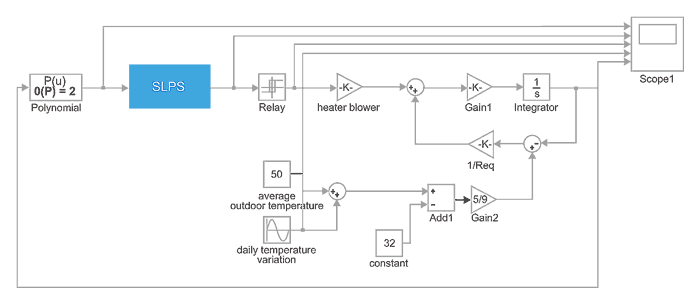
Cadence simulation technology and the MathWorks’ MATLAB Simulink package integrate two industry-leading simulation tools into a powerful co-simulation environment (SLPS). Simulink is a platform for multi-domain simulation and model-based design of dynamic systems. The SLPS integration allows designers to perform system-level simulations that include realistic electrical models of actual components. Design and integration problems can be discovered much earlier in the design process, reducing the number of prototypes needed to execute the design. SLPS integration also lets designers of electro-mechanical systems – such as control blocks, sensors, and power converters – perform integrated system and circuit simulation (See Figure 3.).
Checkpoint restart
This feature allows designer to store simulation states at various time-points and then restart simulations from any of the simulation states, which saves time. Designer can modify simulation settings and design parameters before starting a simulation from a pre-recorded time-state.
Auto-convergence option
This option makes the simulator automatically change tolerances limits of convergence to make the design converge. Designers can use this option to achieve convergence and then fine-tune simulations by further modifying simulator options. This option is recommended for power electronic designs.
Advanced analysis capabilities
Using advanced analysis capabilities, designers can automatically maximize the performance of circuits. Four important capabilities – sensitivity analysis, optimization, Smoke (stress analysis), and Monte Carlo (yield analysis) – enable engineers to create virtual prototypes of designs and maximize circuit performance automatically. Measurements across multiple simulation profiles can be processed together.
Sensitivity
The sensitivity option identifies which component parameters are critical to the goals of a circuit’s performance by examining how each component affects circuit behavior by itself and in comparison to the other components. It allows designers to identify sensitive components and export them to the optimizer to fine-tune circuit behavior.
Optimizer
The optimizer analyzes analog circuits and systems, fine-tuning designs faster than trial-and-error bench testing. It helps find the best component values to meet performance goals and constraints. Designers can use the optimizer to improve design performance, update designs to meet new specifications, optimize behavioral models for top-down design and model generation, and tune a circuit to match known results in the form of measurements or curves. The optimizer includes four engines: least squares quadratic (LSQ), modified LSQ, random, and discrete.
Smoke
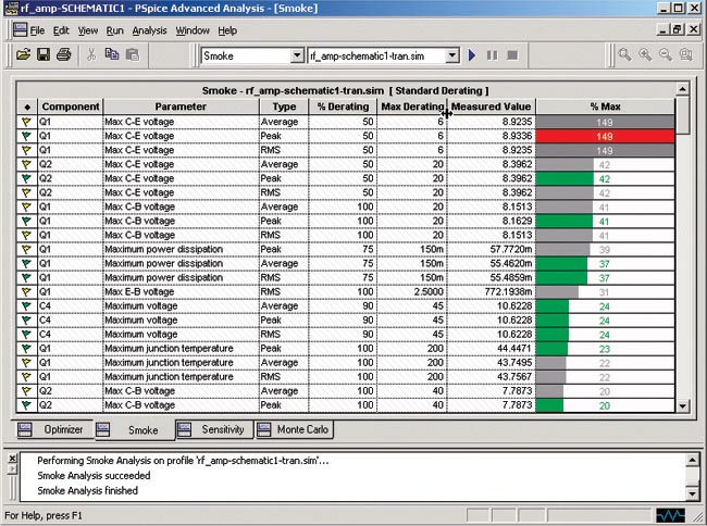
The Smoke option warns of stressed components due to power dissipation, increases in junction temperature, secondary breakdowns, or violations of voltage/current limits. Over time, these components can cause circuit failure. Designers can use Smoke to compare circuit simulation results to a component’s safe operating limits. If limits are exceeded, Smoke identifies the problem parameters. It can also be used for creating, modifying, and configuring derate files for use with Smoke analysis. (See Figure 4.).
 |
|
| Figure 4. | Smoke compares simulated values with manufacturers’ limits to highlight devices operating outside safe operating rages. |
Monte Carlo
Monte Carlo predicts the behavior of a circuit statistically when part values are varied within their tolerance range. Monte Carlo also calculates yield, which can be used for mass manufacturing predictions. Use Monte Carlo for calculating yield based on your specifications calculating statistical data, displaying results in a probability density histogram, and displaying results in a cumulative distribution graph.
Parametric plotter
Once a circuit is created and simulated, the parametric plotter is used for sweeping multiple parameters. Any number of design and model parameters (in any combination) can be swept and results viewed in tabular or plot form. Designers can use the parametric plotter for allowing device/model parameters to be swept, displaying sweep results in spreadsheet format, allotting measurement results in probe UI, and evaluating post-analysis measurement.
System Requirements
- Pentium 4 (32-bit) equivalent or faster,
- Windows XP Professional, Vista Enterprise,
- Minimum 512 MB (1 G or more recommended for XP and Vista Enterprise requirements),
- 300 MB swap space (or more),
- DVD-ROM drive,
- 65,000 color Windows display with minimum 1024 × 768 (1280 × 1024 recommended).
