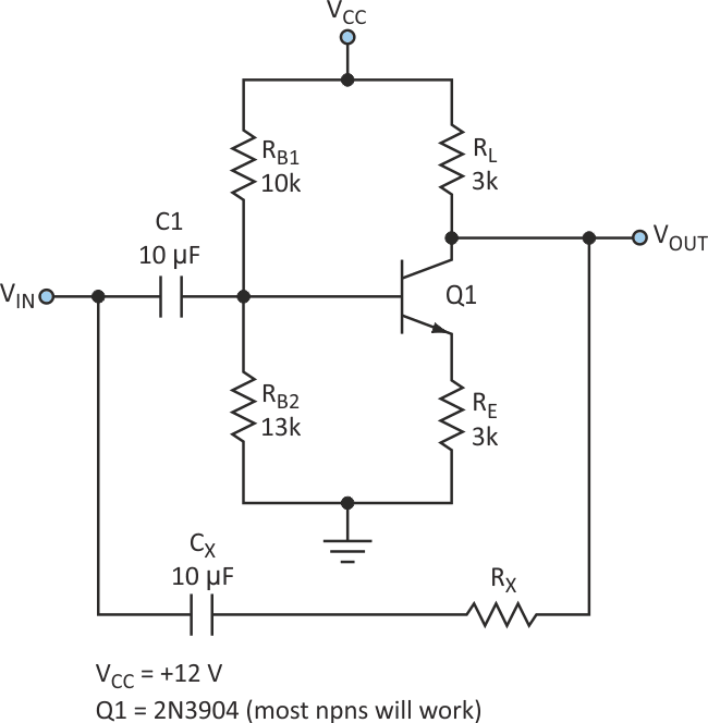
The simple circuit shown accomplishes full-wave signal rectification with only one transistor (Fig. 1). This is done by exploiting the “gain reversal” phenomenon exhibited by a saturated bipolar transistor. This circuit will find applications as a signal-level detector (AGC detector), rectifier, or signal-presence detector.
 |
|
| Figure 1. | By taking advantage of a saturated bipolar transistor’s “gain reversal” phenomenon, this circuit can perform full-wave signal rectification using only one transistor. |
To understand the operation of this circuit, first assume that the transistor is biased in saturation. The bias conditions are established by RB1 and RB2. RL and RE are chosen for the desired gain/dc offset at the output. This circuit configuration is simply a saturated common-emitter (CE) amplifier.
For the following analysis, the component values given are used. Consider a sinusoidal input signal. For a negative-going VIN, VOUT can swing positive. The gain experienced by the signal is about:

(normal operation of a CE stage). However, for a positive-going input signal, the collector-base junction becomes forward-biased (the transistor is saturated) and the transistor operates as an emitter-follower. At this point, the collector is acting as the emitter usually does under forward bias. The gain expression then becomes:
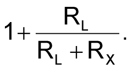
Full-wave rectifier action requires the gain for positive and negative signals be equal in magnitude, but opposite in sign. For a gain of 1, set RX to infinity; this reduces the above equations to:
An npn transistor is used to get a positive-rectified output. Using a pnp transistor (and reversing connections as appropriate) will produce a negative-rectified output. To choose element values, start with the following (for C1, CX coupling capacitors, use as large a value as necessary for the frequency range of interest):
- Ensure saturation: VCC – IC(RL + RE) < VCESAT
- Choose IC.
- Choose RL, RE for desired gain.
- Choose the RB1, RB2 divider consistent with above.
Design for a gain of 1 (RX = infinity) and IC = 2 mA yields: RB1 = 10k; RB2 = 13k; RL = RE = 3k. Gains between 1x and 2x can be achieved, but RX must be included as indicated in the more complex design equations.
 |
|
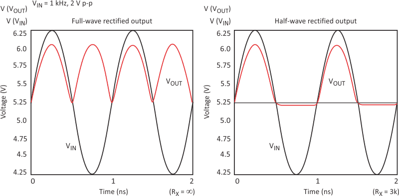
| Figure 2. | A full-wave rectifier is realized by setting RX = ∞. Half-wave rectification is predicted at RX = 3k. |
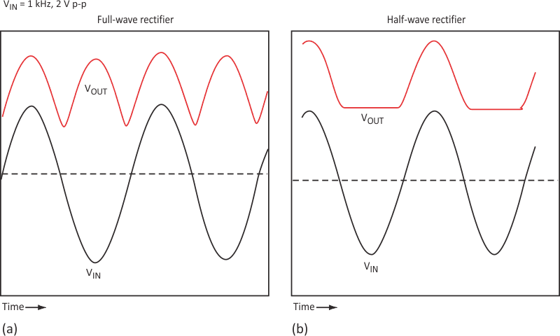
Start with these equations. Iterate with Spice to get optimal values (Fig. 2). This circuit is difficult to simulate accurately due to its inherent nonlinear operation. Thus, performing transient analyses in Spice will produce the best results (Fig. 3). It’s important to have a good transistor model to accurately predict the circuit’s behavior in saturation. Also, including BR (reverse beta) in the Spice models is important because the circuit’s operation relies on reverse operation of the transistor. Check this circuit at higher operating frequencies using Spice transient analyses as well.
 |
|
| Figure 3. | Measured waveforms verify the full-wave (a) and half-wave (b) performance predicted by the Spice analysis. |
A couple of notes to consider:
- Gain is limited to a minimum of 1. Gain scaling and dc offset can be accomplished with a subsequent stage.
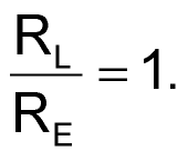
- Use RX as a “symmetry” trim. This will give the rectifier a gain closer to +1 for a positive input. A half-wave rectifier can be made by choosing values that result in
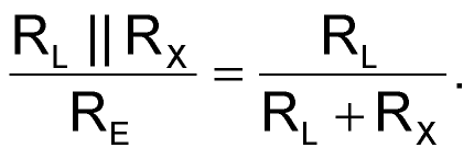
This equality will exactly cancel the positive and negative gains for negative-going half cycles, resulting in half-wave rectification (the transistor will act as an emitter follower only for positive inputs). For the example, RX = 3k will produce a half-wave rectifier.
